
Introduction
PCBs play a critical role by providing electrical interconnections between electronic components, rigid support for mounting those components, and a compact form factor that can be integrated into the final product. They are the primary component in electronic devices responsible for both form and function, enabling advanced semiconductors to communicate with each other at very high data rates.
What is a PCB or Printed Circuit Board?
In short, a Printed Circuit Board consists of a non-conductive substrate, such as fiberglass or epoxy, which provides mechanical support and electrical connectivity to electronic components through conductive pathways etched or printed onto its surface. However, the construction can vary depending on the board type. For example, multilayer PCBs feature three or more conductive copper layers separated by insulating material. These layers interconnect components via traces and pads.
Another example is the HDI PCB, which IPC-2226 defines as a printed circuit board with a higher wiring density per unit area than conventional boards. Compared to traditional PCB technology, they feature finer lines and spaces (≤ 100 μm / 0.10mm), smaller vias (<150 μm) and capture pads (<400 μm / 0.40mm), and a higher connection pad density (>20 pads/cm²). PCBs provide both mechanical support and electrical pathways for components such as resistors, capacitors, and integrated circuits.
What Types of PCBs Exist and What Are They Made Of?
PCBs are composed of conductive and non-conductive layers bonded together. However, the PCB materials used in fabrication and assembly can vary based on the board’s intended application and customer requirements.
Each PCB type utilizes different materials. With this in mind, let’s examine the most popular PCB types in more detail and outline their primary advantages.
Single-Sided PCB
A Single-Sided PCB is a printed circuit board with one layer of conductive material on one side of the board. The other side of the board is used for mounting various electronic components. Single-sided PCBs consist of a substrate layer, a conductive metal layer, a protective solder mask, and a silkscreen layer.
Due to their simple design and cost-effectiveness, single-sided PCBs are very common. Despite a straightforward manufacturing process, they are still used in many complex electronic devices, such as stereo systems, printers, and vending machines.
Double-Sided PCB
Double-Sided PCBs, also known as two-layer boards, allow for more complex designs and circuits.
Unlike single-sided PCBs, double-sided PCBs have conductive copper on both sides of the board. This enables denser routing.
Components on both sides are connected either via Surface Mount Technology (SMT) or Through-Hole Technology (THT), depending on your product’s needs. All the common layers used in single-sided PCBs, such as the substrate, copper layers, silkscreen, and solder mask, are used in double-sided PCBs. However, these are applied to both sides of the board, not just one.
Due to their ease of use and flexibility, double-sided PCBs are highly popular. This is partly because they accommodate more complex circuits, making them suitable for more advanced electronic systems, such as lighting systems and automotive dashboards.
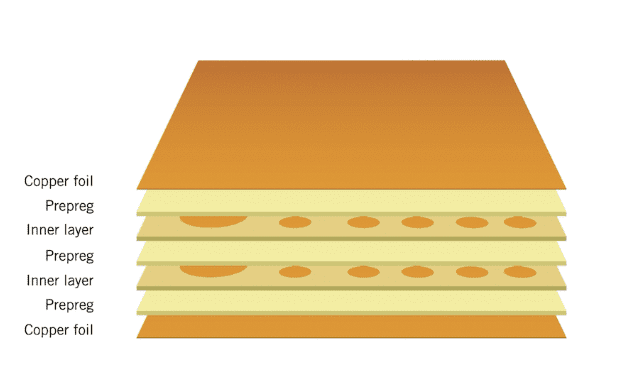
Multilayer PCB
Multilayer PCBs are designed and fabricated using multiple substrate layers. Generally, a multilayer PCB has at least three conductive layers.
These PCBs are constructed using a “sandwich model,” featuring several double-sided conductive layers separated by a corresponding number of insulating material sheets. They are bonded and laminated together under high pressure and heat.
Multilayer PCBs provide greater functionality for computers, medical equipment, GPS trackers, and other complex circuits and devices. In these complex scenarios, they are often preferred over double-sided PCBs because they allow for more intricate circuits within a smaller footprint.
Rigid PCB
As the name implies, Rigid PCBs are solid and inflexible. They are made from several different layers joined together using adhesives and heat. Depending on requirements, rigid PCBs can be single-sided, double-sided, or multilayer.
Rigid PCBs are cost-effective and can be produced in high volumes. They are also highly resistant to wear and tear. Consequently, they are commonly used in products and industries where component stability is crucial.
Flexible PCB
Flexible PCBs, also known as “flex PCBs” or “flex circuits,” are designed to fit within a device or product. Therefore, flexible PCBs are typically thin and light, and they perform very well in tight spaces and around contoured shapes.
Flexible PCBs do not use fiberglass for the substrate layer because it is too rigid. To ensure the board is flexible and durable, flexible PCBs instead use plastics such as Kapton for the substrate layer.
Flexible PCBs are popular because they do not occupy as much space as other PCB forms. They can also withstand extreme temperatures and are compatible with various components and connectors. Most importantly, their inherent flexibility allows them to bend to fit your product.
Rigid-Flex PCB
A Rigid-Flex PCB is a hybrid form of a printed circuit board. It thus combines elements of both flexible and rigid circuit boards. Consequently, rigid-flex PCBs can be folded or flexed continuously. In fact, it is common for the boards to be formed into a bent shape or curve during the manufacturing process.
Rigid-flex PCBs are designed in 3D. This allows the board to be twisted or bent into the desired shape. Most importantly, rigid-flex boards are often thinner than other forms of printed circuit boards. With thin copper layers and adhesive-less laminates, rigid-flex PCBs represent a compact, thin, and lightweight solution.
HDI Printed Circuit Board
HDI PCBs, also known as High-Density Interconnect PCBs, are a relatively new form of printed circuit board. However, they are now one of the fastest-growing technologies in the PCB field.
HDI PCBs possess a higher wiring density per unit area compared to more traditional circuit boards. Furthermore, HDI PCBs feature blind and/or buried vias, as well as microvias with a smaller diameter. This allows designers to place smaller components closer together on the board, enabling faster signal transmission and reduced signal loss or cross-talk.
For these reasons, HDI PCBs are more compact than multilayer PCBs, often with fewer layers. What HDI PCBs may lack in size, they more than compensate for in quality. Consequently, they are popular in advanced technological systems like smartphones and gaming consoles.
LED Printed Circuit Board
An LED PCB is a special type of printed circuit board designed for various lighting modules and applications.
When manufacturing an LED PCB, multiple Light Emitting Diodes (LEDs) are mounted onto a single PCB to form a complete circuit. This allows for full control of their behavior via various switches.
Therefore, LED PCBs are used in countless industries to control lighting. For example, they are used in automotive lighting, street lighting, flashlights, and work lights.
Blank PCB
A Blank PCB is exactly what the name suggests: an empty circuit board without any components mounted to create a functional board.
Due to the visible copper layer, blank PCBs are sometimes referred to as “copper-clad circuit boards.” This copper plays a crucial role. It ensures that when components are placed on the board at a later stage, the board will facilitate an effective and efficient energy flow.
Although some might assume blank PCBs are made entirely of copper, this is inaccurate. To ensure the blank PCB remains durable and robust, silicon and other materials are also used in the process. These also help make the PCB rust-resistant.
Blank PCBs serve as the fundamental foundation for mounting components and parts. These boards are very popular among companies that possess the technology to assemble and manufacture printed circuit boards but require a blank canvas to begin.
Custom PCB
If it better suits your project and needs, we can also offer fully customized solutions in the form of Custom PCBs.
Custom PCBs are now a popular solution. This is especially true if the PCB design needs to be complex, or if the budget requires a balance between labor and manufacturing costs.
A high-quality custom PCB will grant you better control over all aspects of the circuit layout. Furthermore, custom PCBs also tend to appear more professional in the eyes of most industry clients and investors.
Small but Vitally Important
Printed circuit boards account for a relatively small percentage of the total value of the final product. However, they are essential components, critical to the end product – rectifying a faulty PCB is often extremely costly. This makes quality and reliability one of the most important purchasing criteria for our customers.
PCBs Form the Foundation of All PCB-As
The demand for printed circuit boards is primarily driven by the production of PCB Assemblies (PCB-As), as they form the base upon which electronic components are mounted to create the PCB-A. The PCB is the initial component required in the assembly process; without it, neither the PCB-A nor the final product can be manufactured. Furthermore, the circuit board is the sole component to which the customer adds value. Therefore, ensuring high quality of the PCB is paramount, as discarding a PCB-A containing expensive components due to a printed circuit board failure can be very costly.
Applications of PCBs
Medical Devices
From pacemakers and miniature cameras used in minimally invasive surgery to large medical equipment like X-ray machines and CAT scanners, PCBs play a significant role. For instance, flexible and rigid-flex PCBs, with their small size, light weight, and high density, can be used to create more compact and lighter medical devices. For some complex medical equipment, rigid-flex PCBs are an especially ideal choice.
Aerospace
With advancements in aerospace technology, the demand for PCBs in avionics for aircraft, satellites, drones, etc., is also increasing. In these applications, PCBs that are small in size and support complex circuits are typically used. Among these, rigid, flexible, and rigid-flex PCBs are most widely used for instrument panels, flight controls, flight management, and safety systems. Their compact and lightweight design reduces the overall weight of the equipment, thereby lowering fuel consumption requirements.
Consumer Electronics
We can find PCBs in electronic products commonly used in homes and offices, such as computers, smartphones, televisions, home appliances, entertainment systems, and more. These products place high demands on PCBs, including reliability, low weight, and thermal performance.
Industrial Equipment
Most modern industrial equipment is electronically controlled, leading to a continuously growing demand for PCBs across the industry. Equipment such as manufacturing machinery, measurement instruments, power equipment, and robots all require PCBs. Since industrial equipment often operates in harsh environments, PCBs used in industrial settings must be robust enough to withstand chemical exposure, physical shock, high temperatures, and other adverse conditions.
Lighting
Due to their high energy efficiency and longer lifespan, Light Emitting Diodes (LEDs) are becoming increasingly popular across different markets. This has led to a growing use of LED PCBs, particularly aluminum-backed PCBs, which offer better heat dissipation compared to other types of PCBs.
Military and Defense
Military and defense equipment also relies heavily on PCBs, which are essential for vehicles, computers, communication, and surveillance devices. PCBs used in this sector must be extremely durable and reliable, capable of withstanding extreme temperatures and weather conditions.
How is a PCB Manufactured?
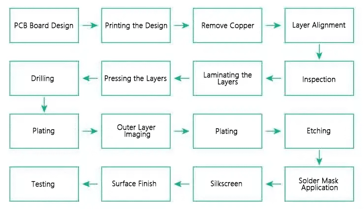
Step 1 – PCB Design
Before manufacturing, the PCB must be designed according to the project requirements. The design is typically completed using computer software such as Altium Designer, OrCAD, or Pads. Once the design is finalized, it is converted into Gerber format, which includes important information like the drill pattern, holes, and component symbols.
Step 2 – Print the Design
The PCB design is printed using a special printer called a plotter. Plotters are characterized by high precision and can display the board’s details and layers, which is very helpful for imaging the PCB. Two ink colors are used in the film: clear and black. For the inner layers, clear ink represents non-conductive areas, while black ink represents conductive copper traces and circuits. For the outer layers, the meanings are reversed.
Step 3 – Remove Copper
To proceed with manufacturing, excess copper must be removed from the board’s inner layers using a copper solvent, leaving the desired copper intact. The amount of copper etchant solvent used can vary; for instance, larger PCBs require more copper to be removed and more time.
Step 4 – Layer Alignment
In this step, the PCB layers are aligned. Both inner and outer layers need to be aligned using an optical punch, which drives pins through punch holes to precisely align the layers of the printed circuit board.
Step 5 – Inspection
Once the inner layers are laminated together, errors cannot be corrected. Therefore, inspection is a critical step. An Automated Optical Inspection (AOI) machine is used to ensure the board is free of defects. Using laser sensors, the machine carefully scans the layers and generates a digital image to compare with the original Gerber file. If any discrepancies are found, the machine displays the comparison for detailed analysis.
Step 6 – Laminate the Layers
First, the layers are secured together using metal clamps, with a prepreg layer placed on the alignment bed. The substrate layer is then placed over the prepreg, followed by a copper foil layer. Additional prepreg sheets are placed on top of the copper layer. Finally, an aluminum foil and a copper press plate complete the stack.
Step 7 – Press the Layers
To press the layers, pins are punched through the stack to maintain alignment. A press machine then applies heat and pressure to the stack, melting the epoxy inside the prepreg and fusing the layers together.
Step 8 – Drill Holes
Before drilling, an X-ray machine is used to locate the drill target points. A computer-guided drill bit then drills holes through the stack. After drilling, a profiling tool removes any excess copper along the panel edges.
Step 9 – Plating
After drilling, the PCB panel is plated. A chemical deposition process fuses all the layers together. The panel is then thoroughly cleaned with other chemical solutions, which deposit a thin layer of copper (about 1 micron) over the panel surface, including the inside of the drilled holes.
Step 10 – Outer Layer Imaging
In this step, a photoresist layer is applied to the outer layer before imaging. This process should be carried out in a cleanroom to isolate the layer surface from contaminants. Ultraviolet light is then used to harden the photoresist, after which any unhardened, unwanted photoresist is removed.
Step 11 – Plating
Similar to Step 9, a thin copper layer is electroplated onto the panel. The panel is then plated with a thin layer of tin. This tin plating protects the desired copper on the outer layer from being etched away in the next step.
Step 12 – Etching
Chemical solutions are applied to remove the unwanted copper. The desired copper, protected by the tin, remains intact. This step establishes the PCB’s conductive areas and connections.
Step 13 – Solder Mask Application
Prior to applying the solder mask, both sides of the panel are cleaned. An epoxy solder mask ink is then applied to coat the panel. Ultraviolet light is used to expose the mask, and the unexposed, unwanted mask is removed. The remaining solder mask is baked in an oven to cure.
Step 14 – Silkscreen
In this step, crucial information (component labels, logos, etc.) is printed onto the board. This is a very important step. Once completed, the PCB panel proceeds to the final coating and curing process.
Step 15 – Surface Finish
Depending on requirements, the PCB can be plated with a solderable surface finish (such as HASL, ENIG, or OSP) to enhance solderability and quality.
Step 16 – Electrical Test
Before the finished PCBs are delivered to the customer, they undergo electrical tests to verify functionality and confirm they conform to the original design.
Summary
You can think of a PCB as the “urban plan” and “foundation” of a modern city:
- Electronic components are like the buildings (residences, malls, hospitals, schools) in the city.
- The PCB itself is the land and foundation, providing a place for the buildings to stand.
- The copper traces on the board are the city’s road system (streets, highways, alleys), responsible for connecting the buildings and allowing vehicles (electrical current and signals) to travel smoothly.
- Multilayer boards are like the city’s overpasses and underground tunnels, enabling complex three-dimensional traffic flow, greatly improving space utilization and traffic efficiency.
Without a PCB, electronic components are just a collection of disparate parts, unable to form a functional system. It is precisely because of the PCB that we can possess such powerful, compact, and diverse electronic products like smartphones, computers, and smartwatches.


0 Comments