
In today’s fast-paced world of electronics, the demand for faster, more reliable communication has never been higher. High frequency PCB (Printed Circuit Board) communication circuits are at the heart of this evolution. From smartphones to satellite communications, these circuits ensure seamless data transmission, making them indispensable in a wide range of applications. Let’s dive into what high frequency PCB are, how they work, and why they are crucial for modern communication systems.
What is a High Frequency PCB?
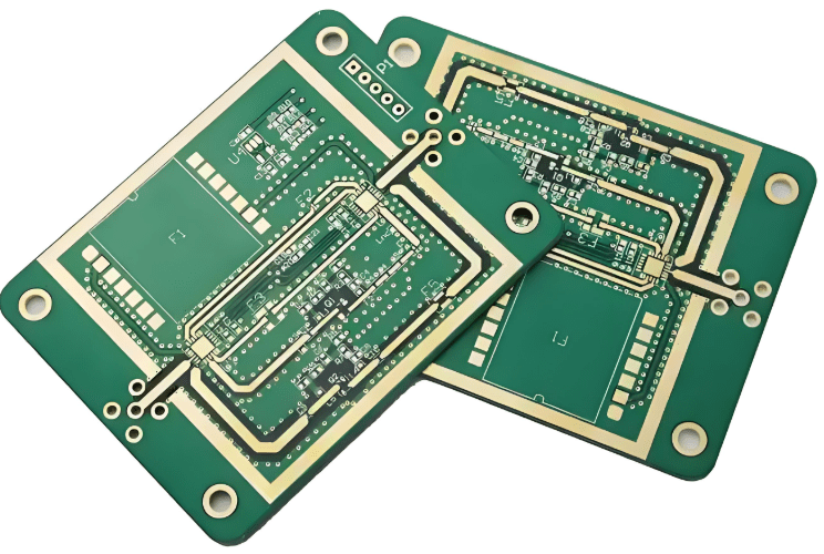
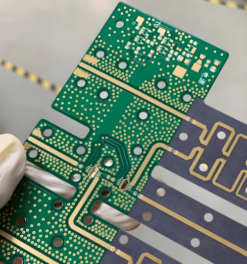
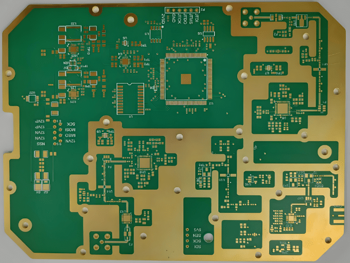
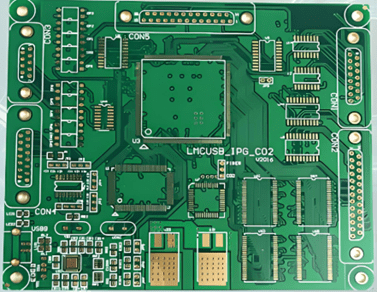
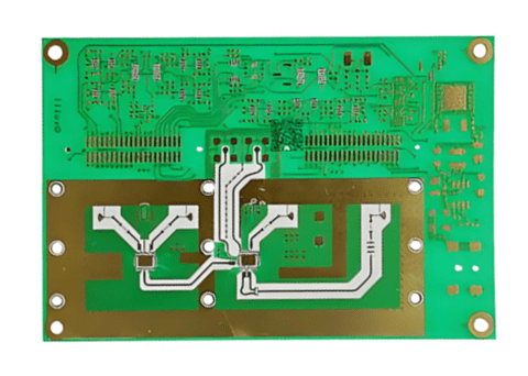
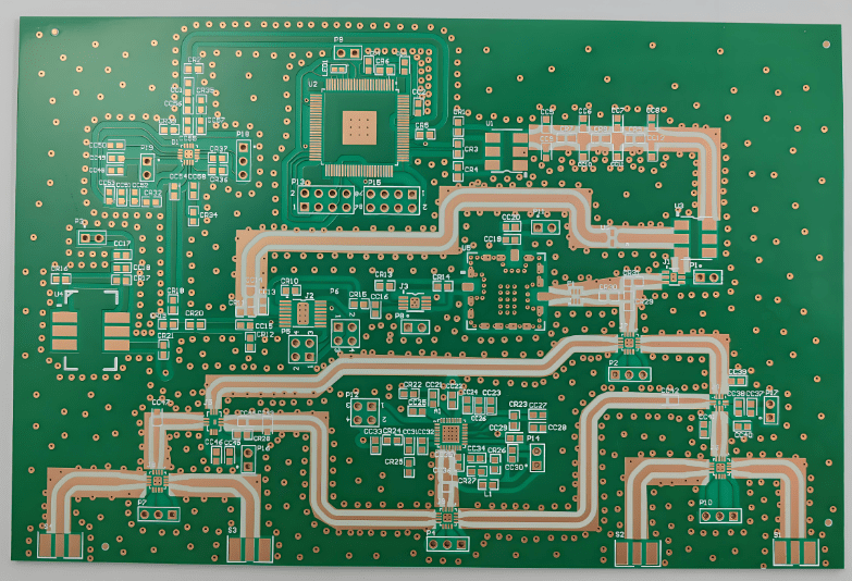
A high frequency PCB refers to a printed circuit board designed to handle and transmit signals at higher frequencies than traditional PCBs. These frequencies typically fall within the radio frequency (RF) spectrum, ranging from several MHz to hundreds of GHz. The key difference between a high frequency PCB and a standard PCB lies in its materials, construction, and performance under high-speed conditions. The design of high frequency PCB focuses on ensuring minimal signal loss, reduced interference, and high transmission speeds. These PCBs often incorporate specialized materials, manufacturing techniques, and careful layout considerations to maintain signal integrity, making them essential for communication applications that require fast and reliable data transfer.
What Are the Types of High Frequency Signals?
High-frequency signals are grouped by frequency ranges and their roles in modern systems. Each range supports different technologies and requires tailored design approaches.
- Low RF (3 MHz – 1 GHz): Found in consumer electronics, broadcasting, and early wireless systems. These signals travel farther and penetrate obstacles more easily, but bandwidth is limited.
- Microwave (1 GHz – 30 GHz): A cornerstone of today’s communication. Used in radar, satellite links, Wi-Fi, and cellular networks. They provide high data capacity but require precise design to reduce loss.
- Millimeter Waves (30 GHz – 300 GHz): The frontier of high frequency use. Essential for 5G, advanced automotive radar, and ultra-fast wireless backhaul. They deliver massive bandwidth, though with shorter range and higher design demands.
Each category has unique strengths and challenges. For PCB designers, frequency range directly guides material selection, trace geometry, and signal integrity control. As frequencies rise, the margin for error decreases, making expertise and advanced materials critical to reliable performance.
What is the frequency range of a high frequency PCB?
A high frequency PCB is built for signals that move far faster than those in standard boards. While a regular PCB may work fine at low MHz ranges, it quickly loses stability at higher speeds. High frequency boards use special materials to reduce loss and keep signals clean. Factors such as dielectric constant, loss tangent, copper finish, and board thickness all shape performance. These details are minor at low speeds but become vital once signals reach hundreds of MHz or into the GHz range.
The frequency range of a PCB depends on its application, material, and design. Consumer electronics may only need MHz operation, while 5G, radar, and aerospace systems demand multi-GHz performance. Understanding this range ensures reliable and efficient communication systems.
- Frequency Range
- Start point: Around 500 MHz, where material effects appear.
- Main range: 500 MHz to 10 GHz, common in wireless, radar, and satellites.
- Advanced range: 10 GHz to 77 GHz+, used in automotive radar and millimeter-wave links.
- Why It Matters
- Cleaner signals
- Lower loss
- Stronger wireless links
- Readiness for new technologies
- Materials and Ranges
| Material | Usable Frequency Range |
| FR4 | Up to ~1 GHz |
| Rogers Laminates | 500 MHz to 10+ GHz |
| PTFE-based Boards | Up to 60 GHz |
| Ceramic-filled | 60 GHz and beyond |
The right material ensures designs meet performance goals.
What is the Material for High Frequency PCB?
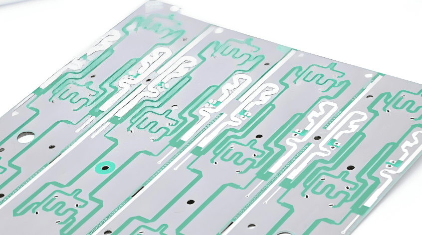
The material used in high frequency PCB plays a pivotal role in their performance. Unlike standard PCBs, which typically use FR4 (a fiberglass-based material), high frequency PCB use specialized substrates designed to reduce signal loss and ensure faster signal transmission.
The most common materials used in high frequency PCB manufacturing include:
- PTFE (Polytetrafluoroethylene): Often referred to as Teflon, this material is known for its low dielectric constant and minimal signal loss at high frequencies. It’s a favorite in RF and microwave applications.
- Ceramic: Ceramic materials offer excellent thermal stability and low signal loss, making them ideal for high-power applications.
- Roger’s Materials: Roger’s Corporation provides a wide range of materials designed for high-frequency applications. These materials offer better performance compared to traditional FR4, with lower loss and improved stability.
- LCP (Liquid Crystal Polymer): LCP is a high-performance material with low loss at microwave frequencies. It’s used in high-speed communication devices like antennas and modules.
The choice of material depends on the specific requirements of the application, such as frequency, temperature stability, and power handling capabilities.
How Does High-Frequency Communication Work?
High frequency (HF) communication works by transmitting signals at specific frequencies across various mediums, whether it be airwaves, cables, or optical fibers. The basic principle is the same: signals are modulated onto a carrier wave, which is then transmitted to the receiver. At high frequencies, the challenges are more significant due to the following factors:
- Signal Loss: High frequency signals are more prone to attenuation, which can reduce the signal strength over long distances. Therefore, careful design is required to minimize this loss.
- Interference: High frequency signals can be easily interfered with by other electronic devices, environmental factors, or nearby circuits. Shielding and grounding techniques are critical in preventing unwanted interference.
- Reflection: At high frequencies, signal reflection can occur at discontinuities in the circuit, leading to signal degradation. Proper impedance matching is essential to prevent this.
Despite these challenges, advancements in materials and PCB design have made high frequency communication more reliable than ever before.
How to Avoid High-Frequency Interference?
High frequency interference can cause significant problems in communication systems, leading to signal loss or degradation. Here are some strategies to mitigate these issues:
- Shielding: Use physical barriers, such as metal shields, to block unwanted signals from interfering with the desired signal.
- Proper Grounding: Ensure that the PCB is properly grounded to reduce electromagnetic interference (EMI) and other noise sources.
- Impedance Matching: Match the impedance of the circuit components to prevent signal reflection and loss.
- Use of Low-Loss Materials: Choosing materials with low dielectric loss can reduce the attenuation of high-frequency signals.
- PCB Layout Considerations: Careful layout design, including minimizing trace lengths and avoiding sharp angles, helps reduce signal loss and reflection.
By applying these techniques, high frequency PCB communication systems can operate efficiently without being negatively impacted by external interference.
High Frequency PCB Impedance Control: Ensuring Signal Integrity at High Frequencies
When working with high frequency PCB, one of the most crucial aspects of the design is impedance control. Impedance control ensures that the electrical signals traveling through the PCB are not distorted or degraded due to mismatches between the source, transmission line, and load. At high frequencies, even small variations in impedance can result in signal loss, reflections, and interference, leading to data errors, decreased performance, and reduced reliability.
Impedance in a PCB refers to the total opposition to the flow of alternating current (AC), which depends on several factors such as trace width, material properties, and the distance between traces. At high frequencies (typically above 1 GHz), maintaining controlled impedance is even more critical because high-frequency signals are more prone to signal degradation and attenuation.
Key Elements of Impedance Control in High Frequency PCB
- Types of Impedance:
Single-Ended Impedance: Refers to the impedance of a single trace relative to ground. In HF PCBs, this is often used for signal transmission lines.
Differential Impedance: Involves pairs of traces that carry complementary signals. Commonly used in high-speed data transmission lines like those found in USB, Ethernet, and DDR memory interfaces.
Controlled Impedance: Ensures that the impedance of the transmission lines is kept constant throughout the signal path to prevent reflections, signal loss, and interference.
- Factors Affecting Impedance Control:
Trace Width and Spacing: The width of a trace and the spacing between traces play a critical role in controlling the impedance. Narrow traces lead to higher impedance, while wider traces lower it.
PCB Material: The dielectric constant (Dk) of the material used affects the impedance. Materials like PTFE (Teflon) or ceramic are preferred in high-frequency applications because they have stable electrical properties at high frequencies.
Trace Length: Longer traces can cause attenuation and signal reflection, so careful attention must be paid to the trace lengths in high-frequency designs.
- Impedance Calculation and Simulation:
Simulation tools like Ansys HFSS, Keysight ADS, and Mentor Graphics HyperLynx are often used in high-frequency designs to simulate the PCB’s impedance characteristics and fine-tune the design before fabrication.
Stackup design and PCB layer configurations need to be considered to ensure that the impedance of traces is consistent across the board.
- Design Rules and Guidelines:
Width-to-gap ratio: The width of the trace compared to the gap between traces is a key factor in determining the impedance. For example, the controlled-impedance traces on a PCB are often defined using design rules like 50-ohm impedance for single-ended traces and 100-ohm differential impedance for pairs of traces.
- Manufacturing Impedance Control:
Impedance control in the fabrication process requires precise etching techniques to ensure that the traces remain consistent in width and spacing. Special attention must also be paid to layer alignment and the quality of the PCB material to minimize any variation in impedance.
Future of High Frequency PCB Communication
The future of high frequency PCB communication is exciting, with a growing need for faster, more reliable data transfer. As we move towards technologies like 5G, 6G, and quantum communication, the demand for high frequency PCB will continue to rise.
- 5G and Beyond: With 5G networks already being rolled out, high frequency communication at millimeter-wave frequencies will become the norm for mobile networks. This will demand more advanced PCBs capable of handling higher speeds and frequencies.
- Quantum Communication: The advent of quantum computing and communication will push the boundaries of high frequency circuits, opening up new possibilities in secure communication.
- Miniaturization: With the increasing demand for smaller, more compact devices, high frequency PCB will become more miniaturized, offering better performance in smaller packages.
- Integration of AI: Artificial intelligence will play a pivotal role in optimizing PCB designs, making high-frequency circuits more efficient and cost-effective.
In conclusion, high frequency PCB communication circuits are integral to the development of future communication systems. As technology continues to evolve, the need for reliable, high-speed data transfer will only grow, ensuring that high-frequency PCBs remain at the forefront of modern electronics.
If you require professional high frequency PCB information or consultation, or if you have any further questions, Thindry PCB is here to assist you.


0 Comments