




Circuit Card Assembly at a Glance
A circuit card assembly (CCA) is a printed circuit board populated with electronic components and soldered interconnections. This guide explains the terminology, process, specifications, inspection methods, testing choices, defects, standards, costs, and manufacturing files that engineers and buyers should define before production.
A circuit card assembly may contain surface-mount devices (SMDs), through-hole components, integrated circuits, connectors, and other electronic parts. Depending on the application, the completed assembly may also require programming, functional testing, conformal coating, or traceability records. These requirements should be defined before manufacturing begins.
What Is Circuit Card Assembly (CCA)?
Circuit card assembly is a populated PCB that combines the bare board, electronic components, and soldered interconnections into a functional electronic unit. The term is common in aerospace, defense, industrial electronics, and other industries where configuration control and documented acceptance requirements may be necessary.
A bare PCB provides conductive traces, pads, vias, and an insulating substrate. After components are installed and soldered, the board becomes a circuit card assembly capable of performing its intended electrical functions.
- Bare PCB: Provides the substrate, copper interconnections, component pads, vias, and solder mask.
- Electronic components: Include resistors, capacitors, diodes, transistors, integrated circuits, and other BOM items.
- Solder joints: Establish electrical connections and mechanical attachment between components and the PCB.
- Connectors and hardware: Provide electrical interfaces, mounting points, shielding, or other mechanical functions.
- Inspection and test records: Document workmanship inspections, electrical tests, functional results, and traceability information.
A completed CCA is not necessarily a fully tested or certified product. Programming, functional testing, coating, enclosure integration, and other operations depend on the agreed manufacturing scope.
Circuit Card Assembly vs. PCBA: What Is the Difference?
Circuit card assembly (CCA) and printed circuit board assembly (PCBA) generally describe the same basic manufacturing result: a PCB populated with electronic components. The terminology varies by industry, organization, and procurement specification.
| Comparison Factor | Circuit Card Assembly (CCA) | Printed Circuit Board Assembly (PCBA) |
|---|---|---|
| Basic definition | A populated electronic circuit card | A PCB populated with electronic components |
| Common terminology | Aerospace, defense, industrial and formal procurement documentation | Commercial electronics, industrial products and electronics manufacturing |
| Assembly methods | SMT, through-hole and mixed technology | SMT, through-hole and mixed technology |
| PCB construction | Rigid, flexible or rigid-flex PCBs may be used | Rigid, flexible or rigid-flex PCBs may be used |
| Quality requirements | Defined by product specification and acceptance criteria | Defined by product specification and acceptance criteria |
| Testing | Electrical and functional testing as specified | Electrical and functional testing as specified |
| Traceability | May require detailed material, lot, serial-number and process records | Depends on customer and product requirements |
| Enclosure integration | Not inherently included | Not inherently included |
Use the terminology in the product specification, drawing package, or purchase contract. Define the deliverables instead of assuming CCA or PCBA automatically includes component sourcing, testing, programming, or final product assembly.
What Components Make Up a Circuit Card Assembly?
The component mix determines the placement process, soldering method, inspection strategy, and potential manufacturing risks. A simple control board may contain resistors, capacitors, and standard ICs, while a high-speed or power-electronics board may require fine-pitch packages, high-current connections, or specialized thermal management.
| Component Type | Common Examples | Main Assembly Considerations |
|---|---|---|
| Passive components | Resistors, capacitors, inductors | Package size, tolerance, orientation where applicable, solder-joint quality |
| Discrete semiconductors | Diodes, transistors, MOSFETs | Polarity, pin configuration, thermal dissipation, soldering requirements |
| Integrated circuits | QFP, QFN, BGA, LGA | Lead pitch, hidden connections, coplanarity, inspection access |
| Connectors | Board-to-board, wire-to-board, RF connectors | Alignment, insertion forces, mechanical support, solder-joint strength |
| Through-hole components | Relays, transformers, large connectors | Hole dimensions, lead fit, solder fill, mechanical loading |
| Electromechanical components | Switches, buzzers, sensors | Orientation, mounting clearance, operating conditions, functional verification |
| Thermal components | Heat spreaders, heatsinks, thermal interface materials | Contact area, thermal resistance, mounting pressure, electrical isolation |
Component selection affects more than BOM cost. Package dimensions, terminal design, moisture sensitivity, thermal limits, and availability influence manufacturing yield and lead time. BGA packages have hidden solder joints that may require X-ray inspection. Polarized capacitors and diodes require correct orientation, while high-current MOSFETs may need sufficient copper area and a suitable thermal path.
Component substitutions should be checked against the approved BOM and design requirements. Similar package dimensions do not guarantee matching electrical characteristics, pin assignments, thermal performance, or qualification status.
What Are the Key Technical Specifications of Circuit Card Assembly?
CCA specifications define the PCB structure, component requirements, soldering process, and acceptance criteria. Values depend on circuit design, operating environment, component datasheets, and reliability targets. The following are common reference examples, not universal manufacturing limits.
| Technical Parameter | Common Reference Values or Options | What to Verify |
|---|---|---|
| PCB layer count | 2, 4, 6, 8, 10 or more layers | Signal routing, power distribution, grounding, stackup |
| PCB thickness | 0.8, 1.0, 1.6, 2.0 mm | Mechanical fit, connector compatibility, rigidity, impedance |
| Copper weight | 0.5, 1, 2 oz/ft² or more (nominal copper areal weight) | Current capacity, thermal rise, trace geometry, finished copper thickness |
| Surface finish | ENIG, HASL, lead-free HASL, OSP, ENEPIG | Solderability, contacts, storage, package compatibility |
| Component package | 0201, 0402, 0603, 0805 (imperial package codes); QFP, QFN, BGA, LGA | Placement accuracy, pad geometry, joint access, inspection |
| Component pitch | 0.4, 0.5, 0.65 mm and package-specific values | Printing accuracy, placement capability, bridging risk, inspection resolution |
| Stencil thickness | 0.10, 0.12, 0.15 mm examples | Paste volume, package mix, aperture design, print consistency |
| Assembly sides | Single-sided or double-sided | Placement sequence, reflow passes, component retention, complexity |
| Solder alloy | SAC305, Sn63/Pb37 or another approved alloy | Regulations, component compatibility, qualified process |
| Reflow profile | Set from solder-paste and component specifications | Ramp rate, soak, time above liquidus, peak temperature, cooling rate |
| Acceptance class | IPC Class 1, 2 or 3, when specified | Product application, acceptance criteria, applicable revision |
| Electrical testing | Flying probe, ICT, boundary scan or functional test | Test access, circuit complexity, coverage, fixtures, pass/fail limits |
How Do PCB Specifications Affect Circuit Card Assembly?
PCB thickness and layer count affect mechanical fit, interconnection density, signal integrity, and fabrication cost. A higher layer count does not automatically produce a more reliable assembly; the stackup must suit the electrical and mechanical requirements.
Copper weight affects current-carrying capacity and heat distribution, but current capacity cannot be determined from copper weight alone. Trace width, finished copper thickness, allowable temperature rise, and the thermal environment must also be considered.
Surface finish influences solderability and contact performance. ENIG provides a relatively flat surface suitable for many fine-pitch packages, while other finishes may be appropriate depending on cost, storage conditions, and application requirements.
How Do Component Specifications Affect Assembly Quality?
Package size and lead pitch influence solder-paste printing and component placement. Smaller components and finer pitches generally require tighter process control, but actual limits depend on package geometry, pad design, stencil configuration, and equipment capability.
Moisture-sensitive components must be stored and handled according to manufacturer specifications and applicable handling standards. Excessive moisture exposure before reflow can damage susceptible packages. The selected reflow profile must meet solder-paste requirements without exceeding component thermal limits.
SMT vs. Through-Hole Assembly: Which Method Is Better?
Surface-mount technology (SMT) places components on surface pads, while through-hole technology (THT) inserts component leads through drilled holes. Mixed-technology assembly combines both approaches on the same circuit card.
| Comparison Factor | SMT Assembly | Through-Hole Assembly | Mixed-Technology Assembly |
|---|---|---|---|
| Component mounting | Components attach to surface pads | Leads pass through PCB holes | Combines surface-mounted and through-hole components |
| Typical components | Resistors, capacitors, QFP, QFN, BGA | Selected connectors, relays, transformers and mechanically loaded parts | Boards with both SMD and through-hole parts |
| Board space | Supports high component density | Requires drilled holes and lead clearances | Depends on component mix |
| Automation | Automated printing, placement and reflow | Wave, selective or manual soldering may be used | Coordinates both technologies |
| Mechanical considerations | Depends on joint design, component loading, PCB support | Can provide useful support for suitable components | Each component needs mechanical and thermal evaluation |
| Inspection | AOI, X-ray where applicable, electrical testing | Visual, solder-joint and electrical inspection | Methods selected for both component types |
| Main challenges | Fine-pitch printing, placement, reflow, hidden joints | Hole fit, solder fill, thermal mass, joint formation | Process sequencing, thermal exposure, inspection access |
SMT is often suitable for compact, high-density circuit cards. Through-hole assembly remains useful for components requiring particular mechanical support or leaded mounting. Mixed technology is common when a board combines fine-pitch ICs with connectors or power components. The best method depends on package design, mechanical loading, thermal dissipation, electrical performance, and production requirements.
How Does the Circuit Card Assembly Process Work?
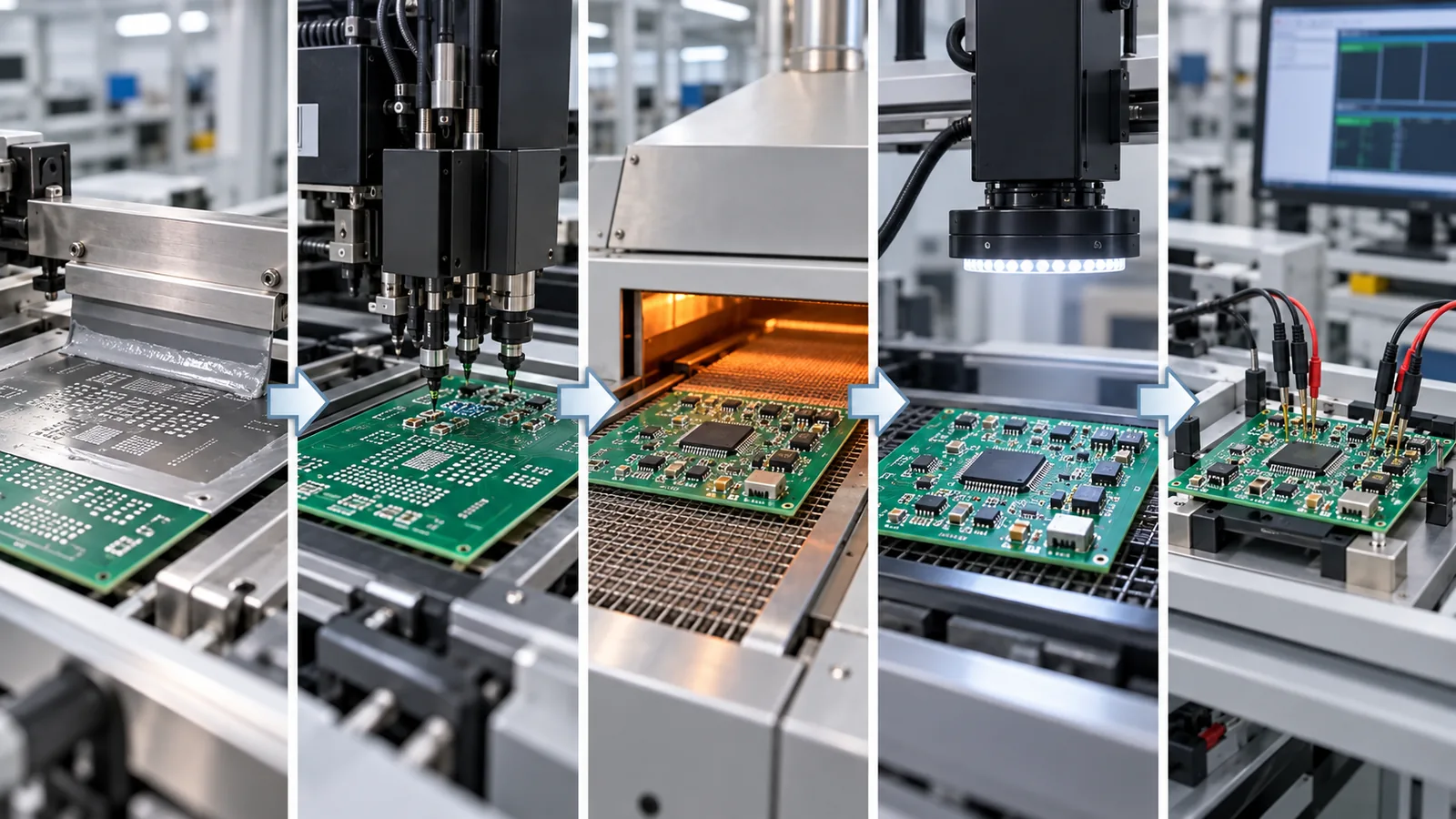
- Review the manufacturing files. Check Gerber or ODB++ data, BOM, pick-and-place coordinates, assembly drawings, PCB revision, and special process notes. Resolve discrepancies before production.
- Verify components and materials. Confirm manufacturer part numbers, package types, quantities, polarity, and approved alternatives. Check moisture-sensitive components, ESD controls, storage, and traceability requirements.
- Prepare the PCB and solder paste. Verify board revision, surface finish, cleanliness, stencil design, and solder-paste condition. Poor paste deposition can cause opens, bridges, and solder balls.
- Place the components. Automated pick-and-place equipment positions components using approved placement data. Fiducials, package orientation, feeder setup, and coordinate accuracy help prevent errors.
- Solder the components. SMT components are commonly soldered using a qualified reflow profile. Through-hole components may use wave, selective, or controlled manual soldering.
- Inspect the assembled board. Use visual inspection, AOI, X-ray, or other suitable methods according to package types and the inspection plan. Document defects and follow an approved rework process.
- Perform electrical and functional tests. Apply specified continuity, isolation, in-circuit, programming, or functional tests. Record results against acceptance criteria and verify the delivered configuration matches the approved revision.
A successful assembly process requires control at every stage. Passing visual inspection does not establish that the circuit functions correctly, and passing a functional test does not prove that every solder joint meets workmanship requirements.
What Are the Most Common Circuit Card Assembly Defects?
CCA defects can originate from PCB fabrication, component handling, solder-paste printing, placement, soldering, or electrical design. Identifying the failure pattern helps determine which process or specification needs attention.
| Defect | Possible Causes | Detection Method | Prevention or Corrective Action |
|---|---|---|---|
| Solder bridging | Excess paste, fine-pitch printing problems, placement errors | AOI, visual inspection, electrical testing | Review stencil apertures, printing alignment, and reflow conditions |
| Insufficient solder | Inadequate paste volume, poor wetting, incorrect joint geometry | AOI, visual inspection, X-ray where applicable | Check paste deposition, pad design, coplanarity, and solderability |
| Tombstoning | Unequal wetting forces, pad geometry, thermal imbalance | AOI or visual inspection | Review land patterns, paste balance, placement, and thermal conditions |
| Component misalignment | Incorrect coordinates, feeder errors, poor fiducial alignment | AOI; X-ray for suitable hidden-joint applications | Verify placement files, machine setup, and board registration |
| Defective solder joints | Inadequate heating, poor wetting, contamination, process variation | Visual inspection and electrical tests | Review soldering profiles, material condition, and process controls |
| BGA solder-joint defects | Paste-printing variation, warpage, placement or reflow issues | X-ray and electrical testing | Control printing, thermal profile, package handling, and inspection criteria |
| Open or short circuits | Solder defects, damaged traces, component faults, assembly errors | Flying probe, ICT, continuity testing, or FCT | Verify PCB integrity, solder joints, orientation, and test coverage |
| Component overheating | Excessive thermal exposure, incorrect polarity, electrical overstress | Visual, electrical, or functional testing | Check component ratings, reflow limits, polarity, and operating conditions |
A defect found during inspection should be traced to its cause rather than simply repaired. Repeated bridging may indicate a stencil or printing problem. Recurring electrical failures may require examination of solder joints, component quality, PCB interconnections, or the test procedure.
Rework must follow an approved method that protects nearby components, PCB pads, and internal layers. Repeated heating or uncontrolled solder removal can introduce additional damage even when the original defect appears corrected.
AOI vs. X-Ray vs. ICT vs. Functional Testing: What Is the Difference?
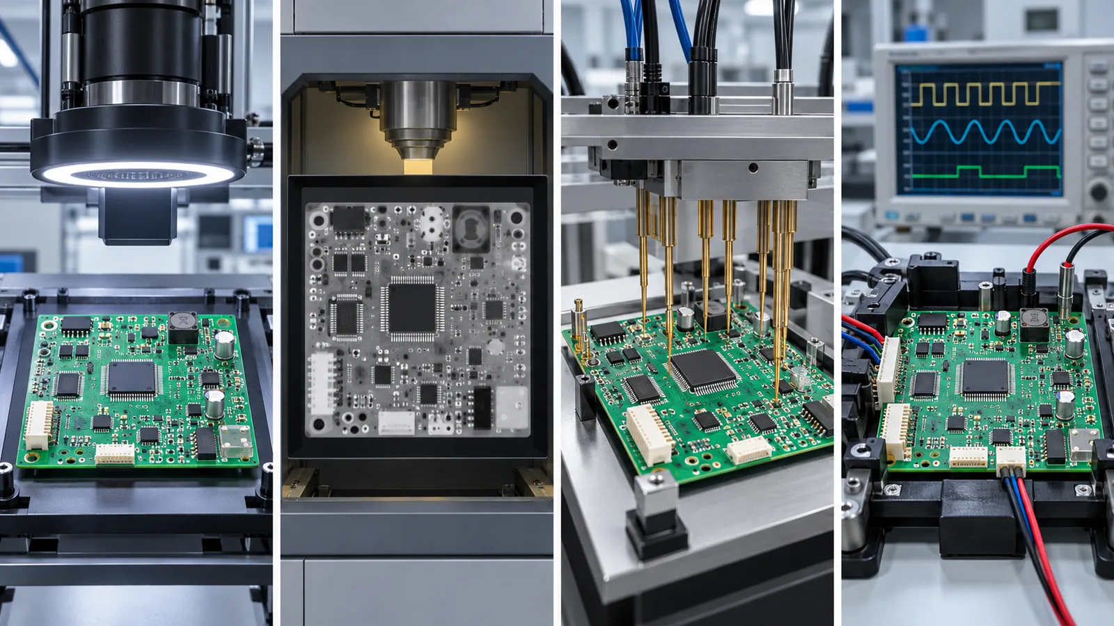
Inspection evaluates visible or internal assembly conditions, while electrical testing checks interconnections or actual circuit behavior. A verification plan should select methods based on package types, failure risks, production volume, and required coverage.
| Method | What It Checks | Main Limitations | Typical Application |
|---|---|---|---|
| AOI | Component presence, orientation, visible placement errors, inspectable solder-joint defects | Cannot directly inspect most hidden BGA joints or prove circuit function | SMT inspection after soldering |
| X-ray | Hidden solder-joint structures, certain bridges, voids, internal assembly features | Requires suitable image interpretation; does not prove function | BGA, QFN and other packages with hidden connections |
| ICT | Electrical conditions at accessible test points, selected opens, shorts, component measurements | Requires test access, coverage planning, often a dedicated fixture | Repeatable production testing |
| Flying probe | Selected electrical connections and component values without a dedicated bed-of-nails fixture | Can be slower than fixture-based testing at high volume | Prototypes, low-volume builds, engineering verification |
| Boundary scan | Supported digital interconnections and device-level test functions | Requires compatible devices, suitable access, and test-program development | Complex digital boards and high-density assemblies |
| Functional circuit test (FCT) | Actual circuit behavior under defined test conditions | Coverage depends on program, fixtures, conditions, and test limits | Power, interfaces, communication, and application functions |
Which Tests Should a Circuit Card Assembly Receive?
The required tests depend on circuit function, operating environment, component packages, and reliability requirements. A practical test plan identifies relevant failure modes, selects suitable detection methods, and defines measurable pass/fail criteria before production.
- Continuity and isolation testing: Verify specified electrical connections and check for unintended shorts between conductors or nets.
- AOI and visual inspection: Check component presence, orientation, polarity, placement, and visible solder-joint conditions.
- X-ray inspection: Evaluate hidden solder joints on BGA, QFN, and other suitable packages when required by the inspection plan.
- ICT or flying-probe testing: Check accessible electrical nodes and selected component characteristics. Coverage depends on the circuit and available test access.
- Functional circuit testing: Verify defined operating functions, such as power-up behavior, communication interfaces, signal response, and input/output operation.
- Environmental and reliability testing: Apply thermal cycling, vibration, humidity exposure, or other stress tests when required by the product specification. These are qualification or reliability tests, not automatic requirements for every production board.
Each test should have documented acceptance limits, equipment requirements, and a defined response to failure. A communication-interface test, for example, should specify the interface configuration, test conditions, expected response, and pass/fail criteria.
AOI, X-ray, and electrical testing are complementary, not interchangeable. AOI identifies visible assembly problems, X-ray can reveal certain hidden-joint defects, and electrical tests identify selected connection faults or verify circuit operation. No single method guarantees detection of every possible defect.
Which IPC Standards Apply to Circuit Card Assembly?
IPC standards can provide a shared basis for soldering requirements and post-assembly acceptance, but the applicable document, revision, class, contract requirements, and product-specific criteria must be agreed before production. IPC released revision J of IPC J-STD-001 and IPC-A-610 in 2024; do not assume that a supplier or purchase order automatically uses the latest revision.
| Standard | Primary Purpose | What to Confirm |
|---|---|---|
| IPC-A-610 | Acceptability of electronic assemblies | Applicable revision, product class, and acceptance criteria |
| IPC J-STD-001 | Requirements for soldered electrical and electronic assemblies | Soldering materials, processes, workmanship requirements, and applicable class |
| IPC-7711/7721 | Rework, modification, and repair of electronic assemblies | Approved rework methods and repair requirements |
| IPC/WHMA-A-620 | Cable and wire harness assembly requirements | Applicability when cable or harness assemblies are included |
IPC-A-610 and J-STD-001 serve different purposes. IPC-A-610 provides acceptance criteria for electronic assemblies, while J-STD-001 addresses requirements for soldered assemblies. They should not be treated as interchangeable documents.
The appropriate acceptance class depends on the intended application and customer requirements. Class 1 generally covers general electronic products, Class 2 covers dedicated-service electronic products, and Class 3 covers high-performance electronic products where continued performance or performance on demand is critical. Specifying an IPC class does not replace electrical performance, environmental, inspection, or product-specific acceptance requirements.
What Affects Circuit Card Assembly Cost?
Circuit card assembly cost depends on more than the number of boards ordered. Component prices, assembly complexity, production volume, inspection requirements, and testing arrangements can all affect the final quotation.
| Cost Factor | Why It Matters | What to Confirm Before Quotation |
|---|---|---|
| PCB complexity | Layer count, dimensions, special materials, and surface finish affect fabrication cost | Final PCB specifications and fabrication files |
| Component count | More placements can increase machine time and process complexity | Complete BOM and placement files |
| Package mix | Fine-pitch ICs, BGA devices, and small passives may require tighter process control | Package types, pitches, inspection needs |
| Sourcing requirements | Availability, lifecycle status, and approved sources affect cost and lead time | Manufacturer part numbers, quantities, substitution rules |
| Assembly technology | SMT, through-hole, mixed technology, and double-sided assembly require different steps | Assembly drawings and process requirements |
| Stencil and tooling | Stencils, test fixtures, and programming arrangements may add initial costs | Prototype quantity, production volume, tooling ownership |
| Inspection and testing | X-ray, ICT fixtures, test development, and records may add cost | Test methods, coverage, acceptance criteria |
| Order quantity | Setup costs are spread across different quantities | Prototype, pilot, and forecast volumes |
| Special handling | Moisture-sensitive devices, coating, and controlled processes may add labor | Handling, coating, and rework requirements |
For a meaningful comparison, request quotations using the same PCB revision, BOM, production quantity, assembly scope, and test requirements. A lower unit price may exclude tooling, programming, component verification, or functional testing, so compare the quoted deliverables line by line.
What Should You Check Before Starting Circuit Card Assembly?
A complete manufacturing package reduces clarification cycles and helps prevent avoidable assembly errors. Verify the following items before releasing an order:
- PCB fabrication files: Confirm Gerber or ODB++ data, drill files, stackup, thickness, copper weight, and surface finish match the approved revision.
- BOM: Include manufacturer part numbers, quantities, reference designators, package information, and approved alternatives.
- Pick-and-place data: Verify component coordinates, rotation, board origin, and orientation conventions.
- Assembly drawings: Identify polarity, reference designators, mechanical hardware, connectors, and special assembly instructions.
- Revision control: Ensure PCB files, BOM, placement data, and assembly drawings correspond to the same released version.
- Component handling: Identify moisture-sensitive devices, ESD-sensitive parts, storage conditions, and special handling requirements.
- Inspection requirements: Specify visual inspection, AOI, X-ray, and other checks required for the component mix.
- Electrical test plan: Define continuity, isolation, ICT, flying-probe, boundary-scan, or functional tests as applicable.
- Acceptance criteria: Specify applicable IPC documents and revisions, product class, and additional customer requirements.
- Traceability and records: Define lot identification, date-code requirements, serial numbers, test records, and material documentation where required.
- Delivery scope: Confirm whether the order includes PCB fabrication, component sourcing, assembly, programming, testing, coating, or final integration.
Resolve discrepancies between the BOM, placement files, assembly drawings, and test documentation before production. If substitutions are permitted, define the approval process in advance rather than allowing unapproved changes during assembly.
FAQs About Circuit Card Assembly
Q1: What does CCA stand for in electronics? A1: CCA stands for circuit card assembly. It refers to a PCB populated with electronic components and assembled to perform a specific circuit function.
Q2: Is circuit card assembly the same as PCBA? A2: In most manufacturing contexts, CCA and PCBA describe the same basic deliverable: a populated PCB. Terminology varies by industry, so the purchase specification should define the manufacturing and testing scope.
Q3: What is the difference between a PCB and a circuit card assembly? A3: A PCB is the bare board with conductive paths and component mounting features. A circuit card assembly includes the installed components and their soldered connections.
Q4: What are the main steps in circuit card assembly? A4: Typical steps include file review, material verification, solder-paste printing, component placement, soldering, inspection, and electrical or functional testing.
Q5: What is the difference between SMT and through-hole assembly? A5: SMT mounts components on surface pads, while through-hole assembly places component leads through drilled holes. The appropriate method depends on package design, mechanical requirements, electrical performance, and production needs.
Q6: What is the difference between AOI and X-ray inspection? A6: AOI examines visible component placement and solder-joint features. X-ray examines internal structures and certain hidden solder-joint defects. The methods serve different purposes and may be used together.
Q7: What is the difference between ICT and functional testing? A7: ICT checks selected electrical connections and component characteristics using defined test access. Functional testing verifies that the circuit performs specified operations under defined conditions.
Q8: What IPC class is required for circuit card assembly? A8: The appropriate class depends on intended use and reliability requirements. IPC Class 1, Class 2, and Class 3 have different acceptance expectations; specify the required class in the purchase documentation.
Q9: What files are required for a circuit card assembly quotation? A9: Common requirements include PCB fabrication files, a complete BOM, pick-and-place data, assembly drawings, quantity, and inspection or testing requirements. Programming files and special process documentation may also be needed.
Q10: How can circuit card assembly defects be reduced? A10: Use consistent manufacturing data, verify part numbers and orientation, control solder-paste printing and soldering, select suitable inspection methods, and define test coverage before production.
Q11: Does every circuit card assembly require X-ray inspection? A11: No. X-ray is particularly useful for certain packages with hidden solder joints, such as BGA devices. Whether it is required depends on package mix, inspection plan, standards, and customer requirements.
Q12: How can circuit card assembly quality be verified before shipment? A12: Review inspection records, electrical and functional test results, defect and rework records, and required traceability documentation. Confirm that the assembly matches the approved revision and acceptance criteria.
Sources and Further Reading
- IPC document revision table
- IPC release of J revisions to J-STD-001 and IPC-A-610
- IPC J-STD-001 endorsement overview
- PCBTRY PCB and PCBA manufacturing overview
Conclusion: How to Specify a Reliable Circuit Card Assembly
A reliable circuit card assembly starts with a complete manufacturing package and clearly defined acceptance criteria. PCB construction, component packages, soldering methods, inspection coverage, and electrical testing must work together to meet product requirements.
Before production, confirm the BOM and assembly files, identify special component-handling needs, select appropriate inspection and test methods, and specify applicable IPC requirements. These steps make quotations easier to compare, reduce preventable manufacturing problems, and provide clearer evidence that the finished circuit card meets its intended requirements.
For a manufacturing review or quotation, send PCBTRY the released Gerber or ODB++ data, drill files, BOM, pick-and-place data, assembly drawings, target quantity, and inspection or test requirements. Contact sales@pcbtry.com or visit PCBTRY to start the review. The review can clarify fabrication and assembly scope, while design authority, product qualification, regulatory compliance, and final acceptance remain with the responsible product team.



0 Comments