




PCB copper roughness describes the microscopic texture of a conductor surface, not the copper thickness or the board’s visible finish. For an RF or fast digital interconnect, specifying a laminate name alone leaves an important part of the loss model unresolved: which foil, which side, and which surface treatment will actually be built?
This guide helps you turn that uncertainty into a supplier question and a test plan. The useful deliverable is a stackup with traceable foil data and an agreed loss check, not a purchase order that merely says “use smooth copper.”
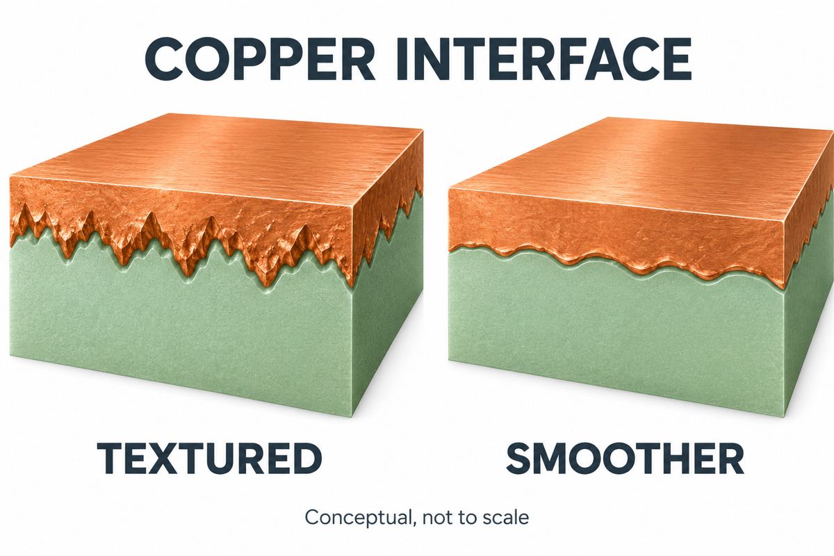
Why does copper roughness affect PCB insertion loss?
At high frequency, current is concentrated near a conductor’s surface. Its texture therefore matters to conductor loss. But the insertion loss you measure through a board also includes dielectric loss, launches, transitions and mismatch. A disappointing S21 result does not identify copper roughness as the cause by itself.
Start with a loss budget: identify the line length, operating band, acceptable attenuation and the transitions included in that allowance. A short feed and a long channel can need different foil decisions even when they use the same material. For digital links, use the channel specification and relevant spectrum, not only the clock frequency.
Samtec’s skin-effect and dielectric-loss presentation provides useful background for separating those mechanisms. The practical question is how much uncertainty remains in your channel after geometry, dielectric and launches have been accounted for.
Standard ED vs low-profile copper: which should you specify?
Choose a documented foil construction, not a label alone. ED means electrodeposited; a low-profile foil can also be electrodeposited. “ED vs low-profile” is therefore a comparison of available foil options, not two mutually exclusive manufacturing methods.
| Option | What to compare | When it deserves review | What not to assume |
|---|---|---|---|
| Standard ED option | Exact foil product and treated-face data | Baseline construction for a channel with adequate measured margin | Every ED foil has the same surface texture |
| Low-profile ED option | Both-face roughness, bonding treatment and compatible laminate | Conductor-loss uncertainty consumes meaningful channel margin | VLP or HVLP names alone specify a universal roughness limit |
| Rolled-annealed option | Actual finish, treatment, construction availability and electrical evidence | The offered laminate and application justify evaluating this alternative | The production method guarantees the finished interface or lowest total loss |
Ask for a quote comparison using the same stackup intent, quantity and validation scope. If an alternative changes dielectric thickness or available copper weight, it is no longer a foil-only comparison. Recalculate geometry and record the change before assigning any measured improvement to roughness.
Also distinguish bare-foil data from the manufactured interface. The MacDermid study on copper roughness measurement discusses measurement settings and bonding treatments. It is a reason to request the test method and processing state, not to reuse historical foil-category numbers as today’s procurement limits.
What do RO4350B LoPro specifications actually tell you?
RO4350B LoPro is a concrete example of a laminate using low-profile reverse-treated ED foil. The Rogers RO4000 LoPro datasheet, pages 3–4, lists the following values.
| Parameter | Published value and condition | Design consequence |
|---|---|---|
| Process Dk | 3.48 ± 0.05; 10 GHz, 23°C, clamped stripline | Do not substitute it blindly for a solver’s design Dk |
| Design Dk | 3.55; 8–40 GHz, differential phase-length method | Confirm applicability to the selected core thickness |
| Dissipation factor | Typical 0.0037; 10 GHz, 23°C | Dielectric loss input, not total PCB insertion loss |
| One listed thickness | 0.0107 in ± 0.0010 in; nominal 0.272 mm | Use the agreed construction tolerance in geometry review |
| Standard claddings | ½ oz: 18 µm; 1 oz: 35 µm | Cladding thickness is not a roughness measurement |
The property table gives typical data, not a finished-board guarantee. Its footnotes state that LoPro bonding resin and core thickness affect the effective design value. Obtain construction-specific guidance. This example does not establish PCBtry inventory or a guaranteed roughness limit.
A useful review response should identify the exact offered construction and attach its governing specification. “Equivalent Rogers material” is not enough to approve a substitution when foil behavior is part of your design assumption.
How should you enter copper roughness in an RF model?
Match the supplied parameter to the selected model before entering a number. Ra, Rq and Rz describe different surface statistics. Keep the reported symbol, units, surface, method and filtering settings together. Do not convert between them with an undocumented multiplier.
- Name the model and software version. In the Ansys Huray implementation documented here, the inputs include nodule radius and surface ratio. A supplier’s Rz value is not automatically either input.
- Map the surfaces. Identify the signal conductor faces and return-plane interfaces represented by the model. Ask separately about plated features; original foil data does not identify a via barrel’s texture.
- Keep an input register. Record the data source, processing state, units, conversion method if validated, and unresolved fields. Mark assumptions as assumptions.
- Run controlled sensitivity cases. Hold geometry and dielectric inputs fixed while varying the supported roughness inputs. Then examine dielectric and geometry tolerances separately.
A model that matches one measurement after arbitrary tuning is not automatically predictive. Retain a second structure or frequency region for checking the fit. Do not hide a launch error inside a roughness adjustment.
What should you ask a PCB manufacturer before approving the foil?
Use this checklist with the fabrication drawing and stackup revision. It makes missing evidence visible before a material substitution reaches production.
| Request | Evidence to retain | Hold point |
|---|---|---|
| Exact laminate and foil designation | Manufacturer, product, copper weight and approved alternative list | A generic “low loss” description cannot close the review |
| Roughness by relevant face | Metric, units, test method, processing state and specification status | Do not compare unlike metrics or typical data with a maximum requirement |
| Final stackup | Dielectric thickness/tolerance, trace geometry, plating and finish | Re-review changes that invalidate the simulated construction |
| Validation coupon | Layer, geometry, length, launches, frequency band and de-embedding plan | A different coupon construction does not validate the intended route |
| Acceptance and change control | Agreed loss criterion, measurement scope, lot traceability and substitution approval | Do not release an unresolved loss requirement as “for reference” |
For example, if a supplier sends “1 µm roughness” without identifying the metric or face, the next action is clarification, not simulation. If it supplies valid data for the original foil but not the bonding treatment, record that remaining uncertainty and decide whether a manufactured coupon is needed.
For the wider manufacturing sequence, use the high-frequency PCB lamination guide. Keep the foil evidence attached to the same approved stackup revision.
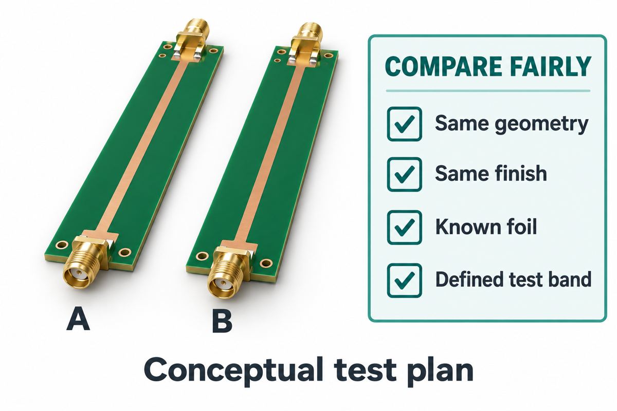
How do you compare measured and simulated loss?
Make the comparison answer one question at a time. A change of laminate, trace width, finish and foil in the same trial cannot isolate the foil’s contribution.
- Define the measurement boundary. State whether connectors and launches remain in the result or are removed through a documented de-embedding method.
- Check the built geometry. Compare actual construction evidence with the simulation assumptions before tuning electrical properties.
- Compare the full band. Inspect insertion loss alongside return loss and phase where relevant, rather than matching one frequency point.
- Explain the residual error. List plausible geometry, dielectric, conductor, finish and fixture contributions. Seek evidence for each rather than selecting the easiest model knob.
- Close the purchasing decision. Approve the construction and acceptance evidence that meet the application requirement. Retain the coupon revision and supplier response for repeat orders.
The primary study Signal Transmission Loss due to Copper Surface Roughness in High-Frequency Region is useful technical background. Its experimental results are not a loss guarantee for a different stackup or manufacturing process.
Copper roughness FAQ
Does a wider trace eliminate copper roughness loss?
No. Changing width changes the transmission-line geometry; it does not change the foil texture. Recalculate impedance with the reference-plane distance and compare total loss. Wider is not an unlimited improvement because routing space, transitions and the intended transmission-line behavior still constrain the design.
Will thicker copper solve the problem?
Not by itself. Copper weight and roughness are separate inputs. A thicker option may also require different geometry or treatment. Ask which construction will be built, then evaluate it against the loss requirement rather than treating copper weight as a substitute for surface data.
Is HVLP always better than standard ED copper?
Not as a complete purchasing decision. Compare the actual offered products, compatible laminate, loss evidence, availability and cost. A category label does not establish your finished-board performance. Use a documented baseline and decide whether the alternative provides needed margin for this application.
Can I use Rz where the simulator asks for Rq or Huray inputs?
Not without a validated mapping. Keep the measurement definition and model definition separate. Ask the laminate or foil supplier for model-compatible data, or document a qualified extraction method. An unlabelled number can produce a plausible-looking curve without representing the manufactured surface.
Is ENIG surface finish the same issue as copper roughness?
No. Finish composition and thickness are additional variables. If the loss comparison changes both finish and foil, its result cannot be assigned only to roughness. Specify the finish on the relevant conductors and include it consistently in the simulation and coupon plan.
Should via barrels use the same roughness data as foil traces?
Do not assume that. A plated barrel and an original foil surface are produced differently. Follow the solver’s feature support and obtain applicable manufacturing data. Where that evidence is unavailable, record the limitation and test its significance instead of silently copying a foil value.
At what frequency must I use low-profile copper?
There is no single frequency that approves every design. Length, geometry, material, loss allowance and manufacturing variation change the decision. Use sensitivity analysis and a representative coupon when margin is tight. A frequency threshold from a forum is not an acceptance specification.
Does a low-loss laminate guarantee a low-loss finished PCB?
No. The foil, completed geometry, finish and transitions also matter. Require the actual stackup and agreed validation evidence. A material datasheet is an input to the design, not proof that a completed board meets the channel’s loss budget.
Request a stackup and foil review
Send your Gerber or ODB++ package, fabrication drawing, proposed stackup, critical-net layers, frequency band, line lengths and loss requirement through PCBtry’s contact page or email sales@pcbtry.com. Attach the checklist above and identify which foil assumptions still need confirmation. Ask for the available construction, any proposed substitutions and the validation scope before approving production.
Material availability, test capability and delivery must be confirmed for the specific project. Do not treat the example laminate parameters in this article as a supplier commitment.



0 Comments