
5G Base Station PCB (5G base station printed circuit boards) are the core hardware foundation for high-speed, low-latency, and high-capacity networks. Design and manufacturing requirements are extremely demanding, requiring not only signal integrity but also impedance control, thermal management, and electromagnetic compatibility (EMC). Leading manufacturers are driving comprehensive upgrades in the 5G PCB industry chain through precision design, advanced processes, and high-reliability materials.
High-Performance 5G Multi-Layer PCB Solutions
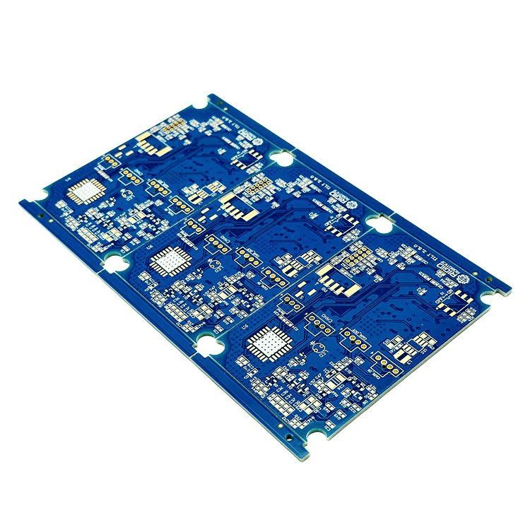
As the circuit complexity requirements of 5G base station equipment continue to increase, 5G multi-layer PCB solutions have become mainstream. High-performance multi-layer PCBs can support higher wiring density and more complex circuit designs within limited space, while also supporting RF modules and improving signal transmission efficiency.
Combining HDI processes, blind and buried via technology, and low-loss high-frequency materials, this solution not only improves PCB reliability and stability but also provides technical support for the efficient collaboration between RF modules, antenna arrays, and data processing units. It is generally believed in the industry that high-performance multi-layer PCBs have become the core support for the rapid deployment and long-term development of 5G networks.
What is the prospect of 5G base station PCB technology?
With the accelerated deployment of 5G networks, 5G base station PCB technology is experiencing unprecedented development opportunities. The market size of 5G base station PCB will maintain rapid growth, becoming a key pillar driving the upgrading of the communications industry.
PCB will move beyond providing electrical connections and move towards higher layer counts and lower losses to meet the demands of high-speed communications.
The application of new high-frequency materials, low-roughness copper foil, and advanced HDI processes will enhance signal transmission performance.
Miniaturization and flexible designs will adapt to various 5G base station deployment scenarios.
These trends will inject new vitality into the communications industry and drive PCB manufacturers to accelerate technological iteration.
Why are 5G base station PCBs so important?
In 5G communication systems, base station PCB are key platforms that carry RF modules, antenna arrays, and data processing units. From market demand to technical implementation, 5G base station PCB demonstrate strategic value in multiple dimensions. Their performance directly determines the network’s signal integrity, transmission efficiency, and operational stability.
Compared to traditional PCB, 5g base station pcb require higher power density, more complex heat dissipation management, and stricter impedance control, resulting in significantly higher technical barriers. Precisely because of this importance, leading global PCB manufacturers are continuously investing in research and development, striving to provide communications equipment vendors with more reliable and high-performance PCB solutions.
The following will address several aspects:
Market Level: Global 5G base station construction is accelerating, driving massive demand for PCBs.
Technical Level: RF signal processing, antenna arrays, and edge computing modules rely on high-speed PCBs.
Industry Level: Upstream material and downstream equipment manufacturers have formed a complete ecosystem.
A comprehensive analysis shows that 5G base station PCBs have become a key link in driving the upgrade of the communications industry.
What challenges does 5G PCB manufacturing encounter?
With the widespread deployment of 5G base stations, 5G PCB manufacturing is also facing technological challenges and upgrades. First, high speed signal transmission requires more precise impedance control; even the slightest deviation can cause signal attenuation or distortion. Second, the high power operation of 5G base stations creates more complex heat dissipation issues, requiring PCB design and material selection to possess superior thermal management capabilities. Furthermore, the use of multi-layer stacking, blind and buried vias, and high-density dielectric (HDI) processes, while increasing circuit density, also increases manufacturing difficulty and cost.
However, beneath these challenges and technological upgrades lie vast market opportunities. Industry insiders point out that manufacturers need to achieve simultaneous breakthroughs in design, materials, processes, and testing to truly meet the high performance PCB requirements of 5G base stations. With the rapid growth of applications such as AIoT, connected vehicles, and smart cities, the 5G PCB manufacturing industry is poised for continued expansion and a new round of technological breakthroughs.
Poor PCB integrity in 5G base stations? A complete troubleshooting guide
During the construction of 5G base stations, PCB signal integrity directly impacts network quality and device stability. Once integrity issues occur, common symptoms include packet loss, increased latency, and even system instability. The causes of these issues may include unstable material dielectric constants, poor routing design, impedance control errors, excessive copper foil roughness, or manufacturing process defects.
To address these issues, industry experts recommend conducting a comprehensive process investigation, from material selection and simulation design to production processes and final testing. For example, using low-roughness copper foil to reduce the skin effect, optimizing trace layout to minimize crosstalk, and performing high-speed signal testing at the final stage are all crucial measures to ensure PCB integrity.
5G Base Station PCB: The Core of Modern 5G Networks
In the entire 5G base station architecture, the 5G base station PCB plays a crucial role, connecting the upper and lower levels. It not only serves as a carrier platform for the RF module, antenna array, and data processing unit, but also directly determines the integrity of signal transmission and system stability. With 5G’s increasing demands for high speed, low latency, and large capacity, base station PCBs must achieve higher-precision impedance control, higher-layer stacking, and more reliable thermal management in their design and manufacturing.
As a professional PCB manufacturer, Thindry leverages its technological advantages in high speed PCB prototyping, multi-layer design, and large-scale manufacturing to provide high-performance solutions to communications equipment manufacturers. It can be said that it is precisely the support of high-performance PCBs that enables the stable operation of 5G networks in application scenarios such as smart cities, the Internet of Vehicles, and the Industrial Internet, earning it the industry’s acclaim as the “core of modern 5G networks.”
Case Study of 5G Base Station PCB in High-Frequency Scenarios
In high-frequency applications, the performance of 5G base station PCBs often directly determines network quality. Taking one of our operators’ 5G base station construction as an example, its design utilizes high-frequency materials with low dielectric constant and low loss, combined with low-roughness copper foil to reduce signal loss during high-frequency transmission. Furthermore, the PCB layout incorporates blind and buried vias and HDI technology, effectively controlling crosstalk while increasing routing density. Practical application results show that this base station maintains stable performance in high-frequency, large-scale data transmission and multi-user scenarios, significantly reducing signal loss.
This case demonstrates that optimized PCB design for high-frequency scenarios is key to ensuring stable operation and efficient coverage of 5G networks.
Summary and Recommendations
With the global deployment of 5G networks, 5g base station pcb have become the core foundation for high-speed, low-latency, and high-capacity communications. From design to manufacturing, from materials to applications, 5g base station pcb are becoming a strategic focus for the communications industry’s upgrade. Despite manufacturing difficulties and challenges, driven by strong global market demand, the industry is accelerating its development towards high performance and intelligent technology.
Faced with the dual pressures of increasing manufacturing difficulties and accelerating market demand, selecting a PCB manufacturer with professional technology and extensive experience is crucial. As a company with many years of experience in the industry, Thindry not only has extensive practical experience in high speed PCB prototypes and 5G base station PCB design and manufacturing, but also provides customers with efficient and reliable complete solutions. We look forward to working with more partners to jointly promote the implementation and application of 5G technology.


0 Comments