
With the rapid development of 5G technology, PCB design has evolved beyond the traditional low-frequency, low-speed design and production phase and has entered a new era of high frequency, high speed, and high density. To help engineers better understand the key points of 5G PCB design, I have compiled a few questions, which we will discuss one by one.
What are the key requirements for high-speed signal transmission in 5G PCB design?
The signal frequencies of 5G systems are typically in the gigahertz range, encompassing low, mid, and high frequency bands. This means that PCB design must ensure the integrity and stability of high-speed signals. Key requirements include the following:
Impedance Control
In high-speed signal transmission, impedance mismatches can cause signal reflections, resulting in eye closure and increased jitter. PCBs must have precise characteristic impedance control, with a typical target value of 50Ω or 100Ω differential.
Signal Integrity Optimization
PCB traces should be kept short and straight, with minimal sharp turns to reduce crosstalk and delay skew. We recommend using differential routing and equal-length control to optimize high-speed links.
Layer Structure Design
Multi-layer PCB structures require rational planning of signal and ground layers to create a continuous reference plane and reduce electromagnetic interference (EMI).
EMI/EMC Control
High-speed 5G signals are more susceptible to radiation, requiring EMI control through ground plane shielding, via fencing, and other methods.
How should 5G high-frequency PCB materials be selected?
5G high-frequency applications present significant challenges in PCB production. The loss of ordinary FR-4 laminates often fails to meet requirements. Therefore, 5G PCB must utilize substrates suitable for high frequencies:
High-frequency signal transmission is affected by dielectric loss. The lower the Dk and Df, the less signal attenuation. For example, high-frequency materials such as Rogers 4003C, Taconic, and Megtron series are widely used in 5G PCB.
Due to 5G’s higher output power, faster speeds, and lower latency, they promote improved thermal management. High-frequency materials must maintain adequate heat dissipation and dielectric constant at high temperatures to eliminate signal loss and prevent PCB breakdown, adapting to the thermal characteristics of high-speed devices.
5G PCB designs utilize both centralized and distributed units, equipped with broadband control units and mobile edge computing. Choosing low-roughness copper foil (LPF, VLP) can reduce losses caused by the skin effect and improve signal transmission efficiency.
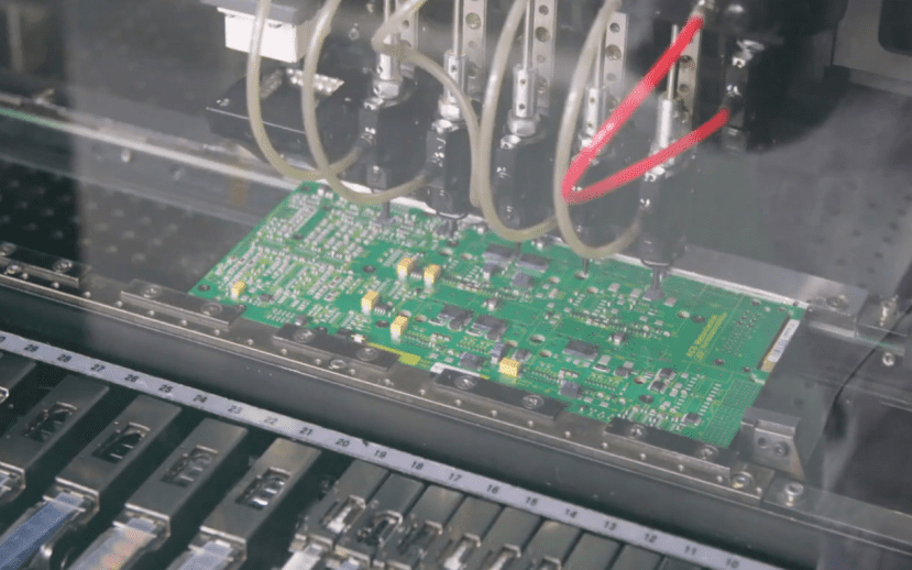
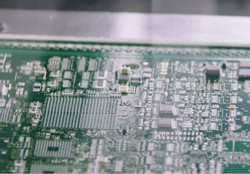
What are the advantages of blind, buried, and microvia technologies in 5G PCB manufacturing?
With the miniaturization and increased functional integration of 5G devices, PCBs must achieve more signal interconnections within limited space. 5G PCB design has introduced blind, buried, and laser microvia technologies. The following discusses the advantages of these technologies.
High Space Utilization
In multi-layer PCB designs, blind vias connect outer and inner layers, eliminating the need for full-board through-hole space and reducing wiring congestion. Buried vias interconnect inner layers without affecting the surface layout.
Signal Path Optimization
Laser microvia technology can shorten the transmission path of high-speed signals, reducing latency and loss, and improving high-speed link performance.
Enabling High-Density Interconnect (HDI)
Blind and buried via technology is the core of HDI boards, enabling 5G PCBs to achieve smaller BGA pad pitches and finer routing designs.
Structural Stability
Filled microvias create a smooth surface, facilitating subsequent SMT processing and improving reliability.
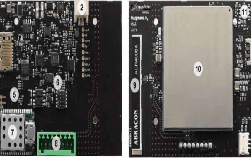
Are there any PCB design examples for 5G devices that we can learn from?
Taking the PCB design of a 5G base station radio unit (RU) as an example, we can see the comprehensive application of 5g pcb design:
Material Selection
A high-frequency substrate and low-roughness copper foil are used to reduce high-frequency losses.
Multi-layer Design
A multi-layer PCB structure with alternating signal and ground layers reduces EMI.
Blind and Buried Via Processing
A 1+N+1 High-density Component Interconnect (HDI) design is used, with laser microvias on the outer layers and buried vias on the inner layers, achieving high-density routing.
Impedance Matching
The RF link is strictly controlled to 50Ω single-ended and 100Ω differential impedance.
Heat Dissipation Design
Plated vias and copper blocks are added below the power amplifier chip to improve heat dissipation efficiency.
This case demonstrates that 5G PCB design is not just about high-speed signal routing; it also requires comprehensive optimization of materials, structure, and process.
What are the advantages of a multi-layer 5G PCB structure? A comprehensive introduction.
In 5G communication systems, data transmission rates and signal frequencies have increased significantly, making single- and double-layer PCB incapable of meeting high-performance requirements. Multi-layer 5G PCB design increases the number of layers to create more routing space, improving both signal integrity and electromagnetic compatibility. Multi-layer boards, through rational design and distribution, reduce the risk of signal interference and crosstalk. Multi-layer PCB offer significant advantages in high-density device integration and miniaturization, providing a reliable hardware foundation for 5G base stations, antenna modules, and RF front-ends.
What are the impacts of 5G PCB trace design?
Trace design in 5G PCB design directly impacts signal transmission quality and system stability. High-speed signal transmission on PCB is susceptible to impedance mismatch, crosstalk, and electromagnetic interference. Therefore, precise trace width, spacing, and stackup must be designed during the early stages of PCB design. Differential pair routing, impedance matching, and equal length control are common design techniques that can significantly reduce signal distortion and latency. At the same time, a reasonable wiring layout can also reduce power consumption, improve heat dissipation efficiency, and provide guarantees for the long-term and stable operation of 5G equipment.
What are the development trends of 5G PCB design?
With the continuous expansion of 5G application scenarios, PCB design is moving towards higher frequencies, lighter weight, and smarter designs. Future 5G PCBs will not only need to maintain signal integrity at high frequencies and high speeds, but also require flexible design and miniaturized packaging to adapt to emerging markets such as wearable devices and smart terminals. At the same time, the use of new materials will gradually become more widespread. For example, substrates with low dielectric constant (Dk) and low dissipation factor (Df) can significantly improve high-speed signal transmission performance. Combined with AI-assisted design and simulation tools, 5G PCB R&D efficiency and reliability will reach new heights.
5G PCB design is a multi-faceted project that requires careful consideration, not only focusing on high-speed signal integrity but also meticulously selecting and optimizing materials and manufacturing processes. Impedance control, material selection, and the application of blind and buried via technology all directly impact the performance and reliability of the final product. If you would like to learn more about 5G PCB design, please Contact US for more product information.


0 Comments