
High-speed communication, real-time data processing, and wireless transmission all rely on one foundational technology: the high frequency PCB. These circuit boards are not your average FR4 boards. They’re engineered to maintain signal integrity at frequencies where even the tiniest loss or delay can disrupt performance.
If you’re working in aerospace, radar, medical imaging, or telecommunications, you’ve probably heard of or worked with high frequency PCBs. But do you know what makes them different? How they work? What materials they use? Or how to design them for maximum performance?
What Is High Frequency PCB?
A high frequency PCB is a printed circuit board designed to carry signals at frequencies above 500 MHz, often reaching into the GHz range. These boards are commonly used in RF (radio frequency), microwave, and high-speed digital applications where timing, impedance, and signal loss are critical.
Unlike standard PCBs, which typically operate in the kHz to low MHz range, high frequency PCBs must deal with effects like skin depth, dielectric loss, EMI (electromagnetic interference), and signal reflections. This means every trace, via, and dielectric layer must be carefully designed and manufactured.
In modern systems—such as 5G antennas, satellite communications, and radar—signal speeds approach the speed of light. At these frequencies, even a small miscalculation can result in signal degradation. High frequency circuit design is not just about layout; it’s about physics, precision, and deep material knowledge.
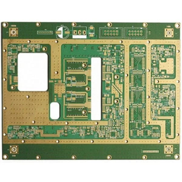
High Frequency PCB Manufacturer
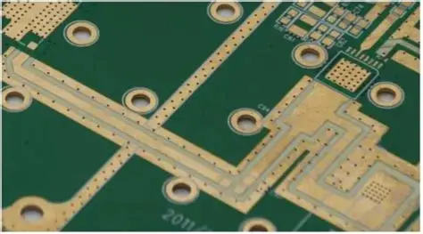
Types of High Frequency PCB
High frequency PCBs come in different structures to meet the requirements of various devices. Here are the three main types:
1. Single-Layer High Frequency PCB
This is the simplest type. It consists of one conductive copper layer on a high-frequency dielectric material like PTFE or Rogers. Single-layer designs are cost-effective and used in basic RF modules or wireless transmitters where complex routing isn’t required.
2. Double-Layer High Frequency PCB
Double-layer boards feature two copper layers separated by a dielectric core. They offer more routing options and better grounding compared to single-layer versions. This structure is suitable for applications such as GPS receivers, RF amplifiers, and wireless routers.
3. Multi-Layer High Frequency PCB
These are advanced structures with three or more layers, often used in aerospace, automotive radar, and high-frequency communication systems. Multi-layer boards provide better signal isolation, reduced EMI, and improved impedance control. The internal ground planes serve as return paths for high-speed signals, minimizing noise and delay.
How Does High Frequency PCB Work?
In traditional low-frequency boards, signals move relatively slowly and electromagnetic effects are minimal. However, in high frequency circuit design, signals behave more like radio waves. They interact with the PCB materials, radiate energy, and are affected by trace geometry and dielectric properties. Here’s what happens:
- Signal Transmission: High frequency signals travel across copper traces. These traces behave like transmission lines, and their impedance must be controlled to avoid signal distortion.
- Dielectric Interaction: The dielectric material (e.g., PTFE, Rogers) directly impacts the signal speed and loss. A low and stable dielectric constant (Dk) helps signals move faster with less distortion.
- Skin Effect: At high frequencies, current tends to flow along the outer surface (skin) of the conductor. This means trace width and copper thickness must be optimized.
- Impedance Matching: If trace impedance doesn’t match the connected components, part of the signal reflects back, causing interference.
- EMI and Crosstalk: Nearby traces can interfere with each other. Proper spacing and shielding are necessary to prevent this.
To sum it up: a high frequency PCB works by maintaining precise signal integrity across every trace and layer. It’s a delicate balance between electrical, thermal, and mechanical design.
Characteristics of High Frequency PCB
High frequency PCBs have specific properties that allow them to operate efficiently in RF and microwave environments. Here are their most important characteristics:
- Low Dielectric Constant (Dk)
- Low Dissipation Factor (Df)
- High Thermal Stability
- Excellent Dimensional Stability
- Controlled Impedance Capability
- High Frequency Performance
Common High Frequency PCB Materials
Choosing the right material is key to success in high frequency design. The wrong choice can lead to signal loss, heat buildup, and system failure. Here are the most widely used materials:
1. Rogers RO4003C / RO4350B
These are the industry standard for RF designs. They provide a low Dk (~3.48), low Df (~0.0037), and stable performance up to 10GHz+. They’re also relatively easy to process with standard PCB fabrication equipment.
2. PTFE (Teflon)
Teflon offers extremely low loss, ideal for systems above 10GHz. It has a Dk around 2.1 and Df below 0.001. However, it’s more expensive and harder to fabricate due to its softness.
3. Ceramic-Filled PTFE
Combines the benefits of PTFE with better mechanical and thermal stability. Often used in aerospace or high-power applications.
4. Polyimide
Used in some high-speed flexible PCBs. Offers better temperature resistance than FR4, but not as good as PTFE for signal performance.
Avoid standard FR4 for high frequency designs. Its Dk and Df are too inconsistent and lead to unacceptable signal loss at frequencies above 1GHz.
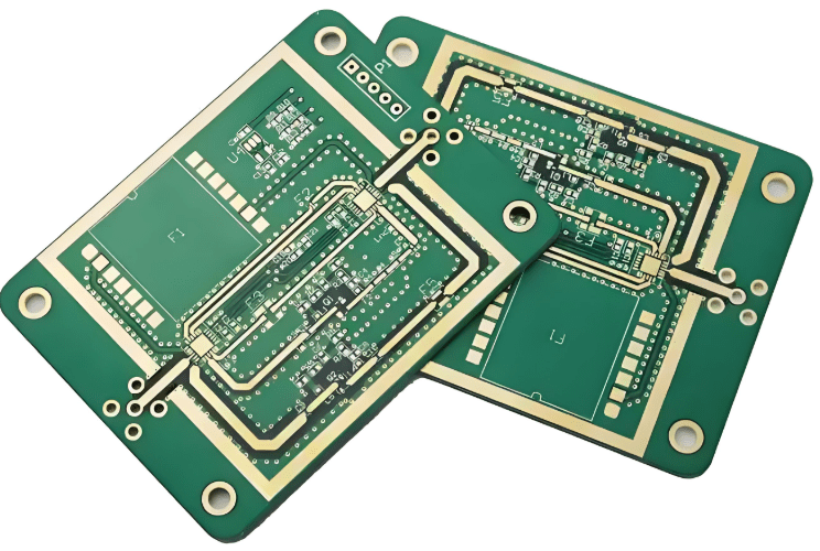
High Frequency PCB Materials
High Frequency PCB Applications
High frequency PCBs are everywhere in modern high-tech industries. If your product involves signal transmission, chances are it uses one. Here are some common applications:
- 5G Base Stations and Antennas: For fast data transfer and signal switching.
- Radar Systems (Automotive and Military): For object detection, navigation, and speed measurement.
- Satellite Communications: Used in uplink/downlink modules and phased-array antennas.
- RF Modules (Bluetooth, Wi-Fi, GPS): Common in smartphones, tablets, and IoT devices.
- Medical Imaging (MRI, CT Scanners): For high-resolution imaging and precision electronics.
- Wireless Routers and Modems: Ensures strong signal transmission in homes and offices.
- Military Communication Devices: Built to handle secure, high-speed transmissions in extreme environments.
High Frequency PCB vs Normal FR4 PCB
Choosing between high frequency PCB and normal FR4 PCB comes down to application needs. If your product involves RF, microwave, or high-speed digital signals, high frequency PCBs are the only viable choice. But if you’re designing consumer electronics, controllers, or low-frequency devices, FR4 is a more economical and practical solution.
At Thindry circuit, we manufacture both types with strict quality standards and offer expert advice on material selection and layout optimization. If you’re unsure which one fits your design, reach out to our engineering team—we’ll help you make the right call. Here is a comparison table between high frequency pcb and normal fr4 pcb.
| Feature | High Frequency PCB | Normal FR4 PCB |
| Dielectric Constant (Dk) | Low (2.2–3.8) | High (~4.5) |
| Dissipation Factor (Df) | 0.0009–0.004 | ~0.02 |
| Frequency Capability | Up to 40GHz+ | <1GHz |
| Impedance Control | Excellent | Poor at high speeds |
| Signal Loss | Very low | High above 1GHz |
| Thermal Stability | Excellent | Moderate |
| EMI Control | High | Limited |
| Fabrication | Complex | Standard |
| Cost | Higher | Lower |
| Applications | 5G, radar, RF | Computers, audio, IoT |
High Frequency PCB Design Guidelines
Designing a high frequency PCB is different from working with standard boards. When signals travel at GHz speeds, even the smallest detail—like a trace bend or via placement—can affect performance. If not carefully managed, your circuit may suffer from signal loss, reflection, or electromagnetic interference.
Here are essential guidelines to follow for successful high frequency circuit design:
1. Control Impedance Precisely
At high frequencies, your traces act like transmission lines. This means the impedance of each trace must be consistent and matched to connected components. Even small mismatches can lead to signal reflection or distortion.
To control impedance:
- Choose a material with a stable dielectric constant (Dk).
- Use impedance calculators to determine the correct trace width, spacing, and layer stackup.
- Maintain consistent dielectric thickness across the board.
- For differential pairs (e.g., USB, HDMI), keep trace lengths and spacing tightly matched.
2. Shorten Signal Paths
The longer the trace, the greater the signal delay and loss. In high frequency design, shorter is always better.
- Keep traces as direct as possible between components.
- Avoid routing high-speed signals around corners or over unnecessary layers.
- Place transmitters and receivers close together to reduce transmission distance.
3. Avoid 90-Degree Trace Bends (Important!!)
Sharp angles in traces, like 90-degree corners, can cause impedance discontinuities. These discontinuities create signal reflections, especially at high frequencies.
Instead, use:
- 45-degree angles for cleaner transitions.
- Rounded trace corners, if possible, for smoother signal flow.
4. Minimize Crosstalk
Crosstalk happens when signals from one trace interfere with another nearby trace. This can be a major problem at high speeds.
To reduce crosstalk:
- Keep a safe distance between parallel traces.
- Use ground shielding or guard traces between critical lines.
- Route adjacent layers orthogonally (i.e., vertical traces on one layer, horizontal on the next).
5. Match Lengths of Differential Pairs
In differential signaling, like USB 3.0, HDMI, or Ethernet, the two traces in a pair must be the same length. If they’re not matched, signal timing will be off, which can cause data errors.
To match lengths:
- Route the two traces together from start to end.
- Use serpentine (zig-zag) routing if needed to balance lengths.
- Maintain consistent spacing between the traces to keep impedance stable.
6. Shield Sensitive Areas
High frequency PCBs are more susceptible to EMI and noise pickup. Shielding helps isolate noisy sections or protect sensitive components.
Options include:
- Grounded copper pour around analog or RF sections.
- Metal shields over RF modules.
- Ground stitching vias near connectors and board edges.
At Thindry circuit, we assist engineers with stackup planning, impedance modeling, and prototyping for all types of high frequency PCB projects. Whether it’s for a 5G antenna, radar module, or RF transceiver, we ensure your board is optimized for speed, stability, and quality.
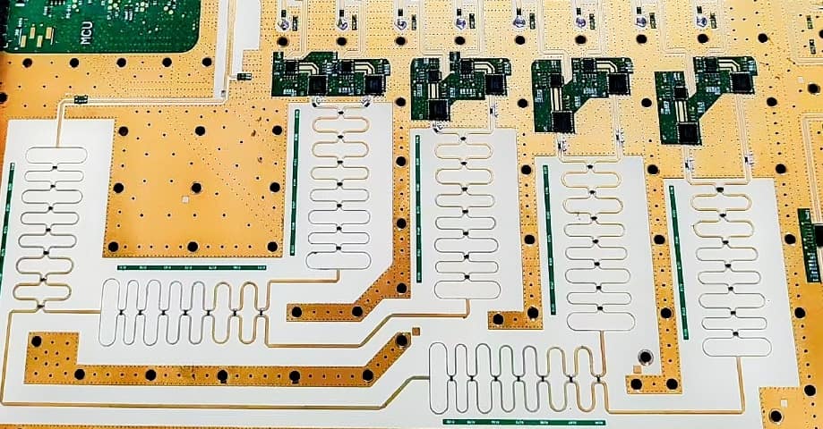
High Frequency PCB Design Guidelines
Considerations During High Frequency PCB Manufacturing
At high frequencies, even minor variations in materials, dimensions, or handling can affect signal integrity. That’s why manufacturers must pay close attention to every step, from material selection to final inspection. Here are key factors that need to be considered during high frequency PCB manufacturing:
1. The most critical part of high frequency PCB manufacturing is using materials with a stable dielectric constant (Dk). Any variation in Dk can cause signal phase shifts or impedance mismatch. Use high-grade materials like Rogers, Taconic, or Panasonic Megtron with tightly controlled Dk values.
2. Because high-frequency signals are sensitive to impedance, trace width and spacing must be fabricated with extreme accuracy. Even a 0.01 mm deviation can lead to unexpected signal reflections.
3. Correct layer stackup is essential for maintaining consistent impedance across high-speed signal paths. The spacing between signal layers and reference planes directly affects performance.
4. At high frequencies, surface roughness impacts signal loss. A smoother copper surface helps maintain signal strength, especially above 1 GHz. Choosing low-loss finishes like ENIG or Immersion Silver, which offer flat and conductive surfaces.
High Frequency PCB FAQs
1. What is the maximum frequency a high frequency PCB can support?
With PTFE or LCP materials, boards can handle up to 40GHz or more.
2. Can FR4 be used in high frequency designs?
FR4 may work up to 500MHz, but it performs poorly above 1GHz due to high dielectric loss.
3. What materials are best for high frequency PCBs?
Rogers RO4350B, PTFE, and ceramic-filled laminates are excellent for high-speed applications.
4. What’s the biggest design challenge in high frequency circuit design?
Maintaining consistent impedance and reducing EMI are the top challenges.
5. Does Thindry circuit offer high frequency PCB manufacturing?
Yes. We provide Rogers, Teflon, and ceramic-based PCBs with impedance control and advanced RF testing.
At Thindry circuit, we offer full support for high frequency circuit design, prototype development, and mass production. We use advanced RF materials, tight process controls, and IPC standards to deliver boards that perform right from the first batch. Need a high frequency PCB that delivers? Contact us now for a free consultation or quote.


0 Comments