
In power electronics, heat and current are the two main challenges. If the copper on a PCB is too thin, the board may overheat or fail. This is where heavy copper PCBs come in. These boards use much thicker copper than standard ones. They can handle more current, spread heat better, and last longer under stress.
At Thindry circuit, we understand the importance of performance, safety, and durability in your circuit boards. Whether you’re working with power supplies, automotive modules, or industrial controls, choosing the right copper thickness makes a big difference.
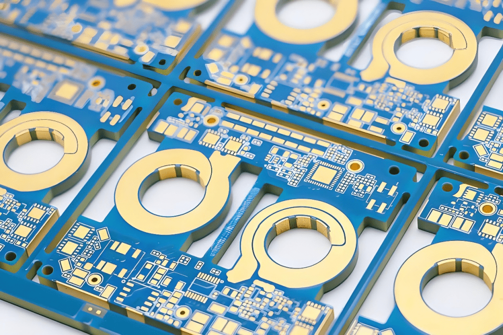
Heavy Copper PCB Manufacturer
What is Heavy Copper PCB?
A heavy copper PCB is a type of printed circuit board with copper thicknesses greater than 3oz per square foot (approximately 105μm). Most consumer-grade PCBs use 1oz or 2oz copper, which are adequate for low-current applications. In contrast, heavy copper PCBs are engineered to handle higher electrical currents, offer improved thermal performance, and increase the board’s mechanical strength.
Copper thickness in PCBs is typically measured in ounces per square foot. Here’s what that translates to:
| Copper Weight | Thickness (μm) | Typical Use |
| 1oz | 35μm | Signal and control circuits |
| 2oz | 70μm | Medium-power electronics |
| 3oz – 10oz | 105μm – 350μm | High-current, industrial use |
| >10oz | >350μm | Extreme environments and high surge conditions |
Heavy copper is used in both single-layer and multi-layer PCBs, particularly for designs requiring power distribution, current balancing, or long-term reliability in harsh environments.
What is Considered Heavy Copper?
In PCB manufacturing standards, any board with copper thickness greater than 3oz (105μm) is defined as a heavy copper PCB. Boards exceeding 20oz (700μm) fall under the category of extreme heavy copper PCBs.
Heavy copper is used not just on outer layers but also on internal layers in multilayer boards. Applications often require precise engineering to balance trace width, spacing, and copper thickness with board manufacturability and electrical performance.
To manufacture heavy copper PCBs, special etching techniques and high-current plating processes are required. So it is better to find a reliable heavy copper PCB manufacturer to ensure highest quality.
Features of Heavy Copper PCB
- Heavy copper PCBs can handle significantly higher currents than standard boards due to their increased copper thickness.
- The thick copper layer improves thermal conductivity, allowing heat to spread efficiently and reduce hotspots.
- Heavy copper PCBs offer stronger plated through-holes and traces, providing better mechanical stability under thermal and mechanical stress.
- These boards can withstand extreme conditions, including high temperatures, thermal cycling, and vibration
- Because heavy copper layers can carry higher current, designers may reduce the total number of layers in a board
- Due to their robustness and thermal durability, heavy copper PCBs tend to have a longer service life, especially in high-stress environments.
What is the Difference Between 1oz and 2oz Copper PCB?
Understanding the difference between 1oz and 2oz copper PCBs is important before exploring heavier options.
| Feature | 1oz Copper PCB | 2oz Copper PCB |
| Copper Thickness | 35μm | 70μm |
| Current Capacity (per trace) | Moderate | High |
| Thermal Conductivity | Standard | Improved |
| Applications | Consumer electronics | Power supplies, LED drivers |
Moving from 1oz to 2oz significantly increases the board’s ability to handle current and dissipate heat. However, in applications requiring even greater current density—such as electric vehicle systems, motor drives, or solar power inverters—a 4oz copper PCB or heavier becomes necessary.
What is the Most Common Copper Thickness in PCB?
The majority of commercially manufactured PCBs use:
- 1oz copper (35μm): Common in signal transmission, control circuits, and general-purpose electronics.
- 2oz copper (70μm): Preferred in medium-power applications like LED drivers, chargers, and industrial sensors.
However, industries that rely on reliable power flow—such as renewable energy, automotive, and military—frequently use 3oz, 4oz, or heavier copper PCBs.
In heavy-duty systems, 4oz copper PCB is often a baseline requirement due to its balance of current handling, heat management, and mechanical strength.
How to Choose PCB Copper Thickness?
Selecting the appropriate copper thickness in a PCB design is essential for ensuring electrical performance, mechanical stability, and thermal reliability. The thickness is typically measured in ounces per square foot (oz/ft²), with common values including 1 oz, 2 oz, and 4 oz copper. For high-current applications, heavier copper—such as 3 oz or 4 oz—is preferred to reduce resistance and manage heat dissipation effectively.
When choosing copper thickness, several factors must be considered:
1. Current load requirements: Higher current requires thicker copper to prevent overheating and voltage drops.
2. Trace width and spacing: Thicker copper allows narrower traces to carry the same current, which is helpful in space-constrained layouts.
3. Thermal management: Applications with high power density, such as power converters or motor drivers, benefit from increased copper to spread and dissipate heat efficiently.
4. Mechanical strength: Boards exposed to mechanical stress or repeated thermal cycling—like in automotive or industrial systems—need the durability of heavy copper.
5. Cost and manufacturability: Thicker copper increases cost and processing complexity, so balance performance with budget and fabrication capabilities.
Proper design tools, such as IPC-2221 standards or online trace width calculators, help engineers accurately determine the required copper thickness based on specific current and temperature rise constraints.
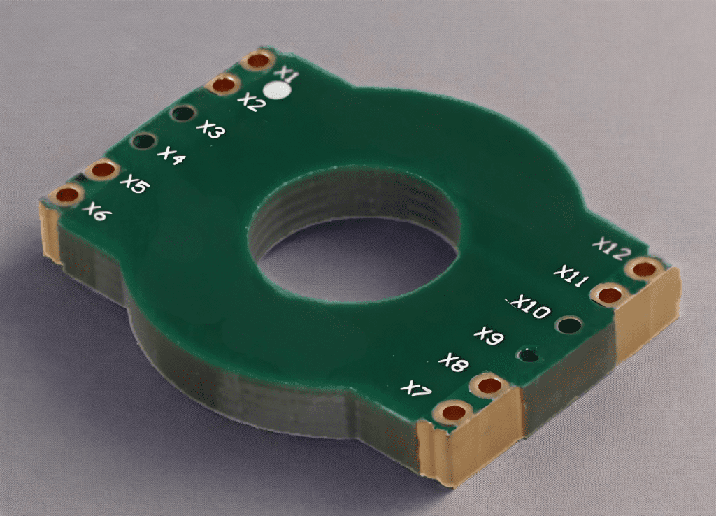
Extra Heavy Copper PCB Made by Thindry
Heavy Copper PCB Design Guide
Designing a heavy copper PCB involves more than simply selecting a thicker copper layer—it requires careful attention to thermal dynamics, mechanical integrity, and manufacturability. Heavy copper PCBs typically use 3 oz to 20 oz of copper per layer and are widely used in power electronics and high-current applications.
1. Layer Stack-up Considerations
Designers should work with the manufacturer early in the process to define an optimal layer structure. Heavy copper layers can be used selectively (e.g., on power layers only) to reduce costs and maintain design flexibility. It’s important to ensure that dielectric materials and prepregs can withstand the heat and stress associated with heavy copper etching and plating.
2. Trace Width and Spacing
Due to increased copper volume, trace width and spacing must be recalculated using IPC-2152 guidelines. Wider traces and adequate spacing are essential to accommodate higher current without compromising insulation integrity.
3. Plated Through Holes (PTH)
Drill size and aspect ratio must be optimized, as heavy copper requires deeper plating in vias. This ensures reliable conductivity and mechanical strength across layers. It also prevents barrel cracking during temperature fluctuations.
4. Thermal Management
Heavy copper helps distribute heat effectively, but heat sinks or thermal vias might still be needed in high-power sections. Copper pours, planes, and dedicated heat zones should be strategically placed to optimize thermal pathways.
5. Mechanical Stress Resistance
For environments with vibration, shock, or wide temperature ranges, heavy copper provides the physical robustness needed. However, designers must also consider board thickness and flexural strength when assembling complex systems.
6. Cost vs. Benefit Optimization
While heavy copper increases material and processing costs, the performance improvements often outweigh the expense in high-reliability sectors such as military, aerospace, automotive, and industrial power management.
Heavy Copper PCB Applications
Heavy copper PCBs are used in industries where high power density, reliability, and thermal stability are essential. Common applications include:
- Power Electronics – AC-DC converters, DC-DC modules, and power inverters for reliable energy transfer and heat management.
- Automotive Systems – Found in engine control units, EV battery systems, and onboard chargers where high current and durability are required.
- Industrial Equipment – Used in motor drives, factory automation, and high-current controllers that demand robust PCBs with minimal downtime.
- Medical Devices – In surgical, imaging, and diagnostic equipment.
- Aerospace & Defense – In avionics, radar systems, and satellite control circuits where mechanical and thermal reliability is critical.
- Renewable Energy – Used in solar panel inverters, wind turbine controls, and battery management systems for reliable and efficient energy processing.
Frequently Asked Questions (FAQs)
1. What is the thickest copper available for PCBs?
Thindry circuit can manufacture boards with up to 20oz copper. For custom requirements above that, contact our engineering team.
2. Is a 4oz copper PCB standard for industrial power systems?
Yes. A 4oz copper PCB is commonly used in power-intensive applications such as converters, inverters, and automotive modules.
3. How does copper thickness affect trace width?
Thicker copper allows for narrower traces to carry the same current, which is useful in space-constrained designs.
4. Can I use heavy copper in multilayer PCBs?
Yes. Heavy copper can be used on outer and inner layers. Proper stack-up design is essential for layer balance and manufacturability.
5. What is the typical lead time for heavy copper PCBs?
Lead time depends on layer count and copper weight. For 4oz–6oz copper, standard lead times are 7–15 working days, with expedited services available.
Heavy copper PCBs offer a practical and reliable solution for high-current, high-temperature, and mechanically demanding environments. From 4oz copper PCB designs to extreme heavy copper builds, these boards support the next generation of power electronics.
Selecting the right copper weight is not just about thickness—it’s about aligning your performance needs with professional design and manufacturing capabilities. With Thindry circuit, you gain a dependable partner backed by certifications, advanced fabrication techniques, and industry expertise. Ready to start your heavy copper PCB project? Contact Thindry circuit for design consultation or to request a quote today.


0 Comments