
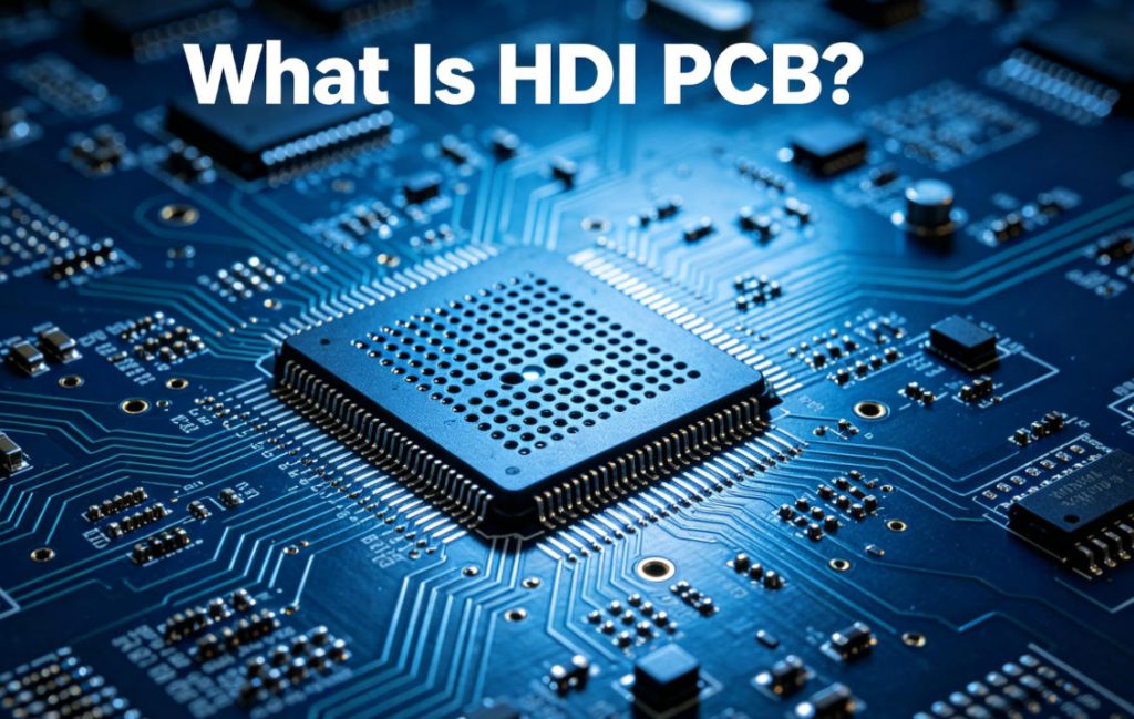
What Is HDI PCB and How Does It Work?
Understanding what is HDI PCB allows hardware designers and sourcing professionals to select optimal circuit boards for compact, high-performance electronic devices, and mastering what is HDI PCB core technology helps avoid common specification errors in advanced PCB development. HDI PCB, short for High Density Interconnect PCB, is a premium circuit board fabricated with laser microvia, blind hole, and buried hole technologies to support ultra-fine, high-density wiring layouts.
Unlike conventional PCBs that rely on bulky mechanical through-holes, HDI PCBs utilize precision laser-drilled microvias to connect internal circuit layers.
This innovative structural design maximizes wiring capacity within limited board space and delivers cleaner, faster signal transmission for modern miniaturized electronics.
What Core Features Define a Standard HDI PCB?
Standard HDI PCBs are uniquely defined by microvia structures, ultra-fine line geometries, and high layer density, serving as the key differentiators from conventional multilayer PCBs. These core technical features directly determine the board’s miniaturization potential and high-frequency electrical performance for premium electronic applications.
Key Technical Characteristics
- Laser-drilled micro blind and buried vias that create smaller, space-efficient layer connection points
- Ultra-fine line width and spacing under 0.1mm, enabling dense component and circuit layout
- Precision sequential lamination structure that supports reliable multi-layer board stacking
- Shorter signal trace paths that effectively reduce signal transmission loss and time delay
- Elevated pad density that accommodates compact surface-mount packaged components
What Is the Difference Between HDI PCB and Regular PCB?
HDI PCB outperforms regular PCB in wiring density, space utilization efficiency, and high-frequency signal stability, making it indispensable for modern miniaturized high-speed electronics. Traditional regular PCBs use standard through-hole technology that wastes valuable board space and causes severe signal attenuation in high-frequency operating environments.
| Parameter | HDI PCB | Regular PCB |
| Via Type | Laser-drilled micro blind/buried vias | Traditional mechanical through-holes |
| Line Width & Spacing | Ultra-fine (0.075mm–0.1mm) | Standard (≥0.15mm) |
| Wiring Density | Extremely high, ideal for compact circuit layouts | Limited capacity, causing unnecessary space waste |
| Signal Performance | Low signal loss, minimal crosstalk, high operational stability | Noticeable signal delay and electromagnetic interference |
| Application Scenarios | High-end compact, high-speed electronic devices | Basic low-speed industrial and consumer electronics |
What Are the Main Benefits of Using HDI PCB?
HDI PCB solves critical pain points of traditional PCBs, including insufficient layout space and poor high-frequency performance, while greatly enhancing product miniaturization, signal quality, and structural stability. It allows hardware developers and manufacturers to boost product competitiveness without increasing overall device dimensions.
Performance & Structural Advantages
- Enables ultra-thin, lightweight device designs suitable for portable consumer electronics
- Minimizes high-frequency signal loss and crosstalk interference for high-speed circuits
- Enhances structural rigidity and effectively reduces board warpage and deformation risks
- Supports high-density chip packaging formats such as BGA and QFN
- Improves long-term operational stability and extends electronic product service life
What Popular Industries Use HDI PCB Applications?
HDI PCB is widely adopted in high-precision industries that demand miniaturization and high-speed signal transmission, resolving the core conflict between compact device size and complex functional circuitry. Four mainstream industries feature mature, large-scale HDI PCB application cases.
Consumer Electronics
HDI PCB is extensively used in smartphones, TWS earbuds, and smart wearable watches. It integrates dense control and sensing circuits on ultra-thin boards, enabling lightweight, portable product designs while maintaining complete functional performance.
Communication Equipment
It serves core components of 5G base station modules, signal transceivers, and portable communication terminals. The optimized layout shortens high-frequency signal paths, reduces signal attenuation, and ensures stable high-speed data transmission.
Automotive Electronics
HDI PCB is deployed in vehicle smart displays, ADAS sensing modules, and automotive main control units. It adapts to extreme temperature fluctuations and vibration environments, delivering reliable high-density circuit support for intelligent automotive systems.
Medical Electronics
It applies to portable diagnostic devices, wearable medical monitors, and miniature therapeutic instruments. Its high-precision wiring and stable electrical performance meet strict medical industry safety and reliability standards.
What Design Rules Must Follow for HDI PCB Projects?
HDI PCB design requires stricter precision specifications than conventional PCBs to avoid manufacturability defects and performance degradation. Adhering to standardized design guidelines ensures full DFM compliance and stable mass-production yield rates.
Critical Design Guidelines
- Standardize microvia size and depth parameters to prevent drilling deviation and interlayer short circuits
- Isolate high-speed signal traces from power traces to suppress crosstalk interference
- Maintain uniform line width and spacing to eliminate open-circuit and short-circuit risks
- Optimize component layout to balance board stress distribution and reduce warpage
- Reserve adequate solder mask clearance for high-density pad areas to ensure smooth assembly
What Common HDI PCB Types Are Available for Projects?
HDI PCBs are categorized by lamination structure and microvia distribution, with each type matching specific precision and application requirements. Selecting the appropriate HDI PCB type prevents over-engineering or insufficient performance for project demands.
Main HDI PCB Classifications
- Single-sided HDI: Features microvias on one layer only, ideal for simple compact consumer electronic devices
- Double-sided HDI: Equipped with microvias on top and bottom layers, suitable for medium-precision functional modules
- Multilayer HDI: Adopts multi-layer stacked lamination, designed for high-end communication and automotive electronic equipment
- Any-layer HDI: Supports full interlayer microvia connectivity, customized for flagship high-precision electronic products
What Manufacturing Challenges Do HDI PCB Designs Face?
The high-precision structure of HDI PCB brings higher manufacturing difficulty, and unoptimized design files frequently cause low yield rates and production delays. Most manufacturing defects stem from non-standard microvia design and unreasonable layer stacking configurations.
Frequent Manufacturing Pain Points
- Microvia position offset and incomplete drilling caused by inaccurate design parameter settings
- Uneven copper foil thickness leading to inconsistent electrical conductivity
- Layer alignment deviation occurring during multi-layer lamination processes
- Insufficient trace and pad spacing triggering short circuits after copper plating treatment
How to Optimize HDI PCB Performance for High-Speed Devices?
Targeted optimization of HDI PCB layout and stacking structure can significantly improve high-speed signal stability and anti-interference capability. Minor design adjustments effectively resolve most high-frequency signal loss and noise interference issues in precision electronics.
- Implement complete ground plane pouring to isolate external electromagnetic interference
- Optimize microvia placement positions to shorten high-speed signal transmission paths
- Configure precise impedance matching for high-frequency traces to reduce signal reflection
- Disperse heat-generating components evenly to avoid local overheating and performance degradation
How to Verify HDI PCB Design Feasibility Before Production?
Pre-production feasibility verification eliminates hidden design flaws and ensures seamless mass production of HDI PCBs. Comprehensive inspection covers design rule compliance, manufacturing limitations, and electrical performance compatibility.
- Perform strict DRC checks to verify line spacing, microvia dimensions, and layer parameters
- Validate lamination stacking sequence to avoid structural conflicts and layer mismatches
- Simulate high-speed signal integrity and impedance matching performance
- Confirm pad size and layout compatibility with standard SMT assembly processes
FAQ: Common Questions About HDI PCB Design & Manufacturing
Q1: What exactly does HDI PCB mean in electronics?
A: HDI PCB stands for High Density Interconnect Printed Circuit Board. It is an advanced high-precision circuit board that uses micro blind and buried via technology to achieve ultra-high wiring density, supporting the miniaturization and high-speed performance of modern electronic products.
Q2: Are HDI PCBs more reliable than regular PCBs?
A: Yes. HDI PCBs feature shorter signal paths, lower electromagnetic interference, and stable layered structures. They deliver superior long-term reliability, especially for high-frequency, portable, and vehicle-mounted electronic devices.
Q3: What projects need to use HDI PCB instead of regular PCB?
A: Any project requiring ultra-thin form factors, high-density component integration, and stable high-speed signal transmission requires HDI PCB. Typical applications include smartphones, 5G communication modules, automotive intelligent systems, and portable medical devices.
Q4: Can beginners design HDI PCB files successfully?
A: Beginners can complete basic HDI PCB design after mastering microvia design rules and layer stacking standards. Professional pre-production DFM inspection is still essential to fix potential manufacturability risks.
Q5: What is the biggest advantage of HDI PCB for product iteration?
A: HDI PCB enables manufacturers to achieve product miniaturization and performance upgrades without expanding device size, supporting faster iteration of compact, lightweight, and high-performance electronic products.
Professional HDI PCB Customization & Manufacturing From Thindry
Whether you need prototype validation or mass production of high-precision HDI PCB, professional manufacturing support ensures your design meets strict industrial performance and yield standards. Unoptimized HDI designs often result in production failures and compromised device performance.
We support on-demand customization of all types of HDI PCBs and high-density multilayer circuit boards for consumer electronics, communication, automotive, and medical industries.
Our professional engineering team provides free DFM reports to detect potential design flaws, optimize layer stacking, microvia layout, and wiring schemes, and eliminate manufacturing risks in advance.
From rapid prototyping to large-scale batch production, we deliver high-yield, stable HDI PCB solutions. For technical inquiries and order cooperation, feel free to contact our official email: sales@pcbtry.com.

0 Comments