
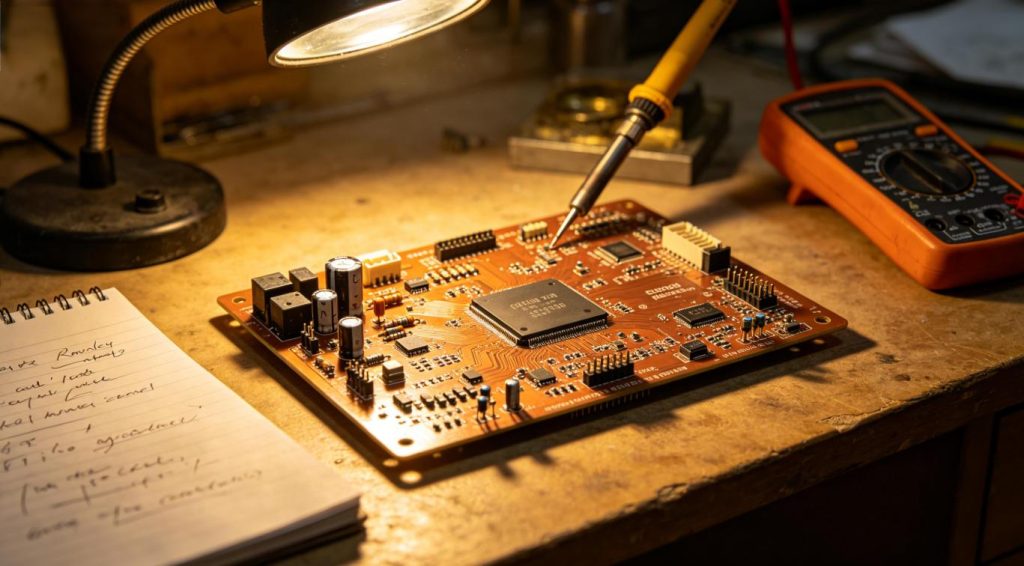
What Is the Simplest Way to Design a PCB for Beginners?
You can easily learn how to design a PCB for beginners by following a standardized workflow, and understanding how to design a PCB for beginners helps you avoid technical errors and manufacturing failures.
Beginners should start with simple schematics, basic layout rules, and free design software instead of complex multilayer boards.
Keep your first project minimal to build stable design habits and improve layout intuition.
What Basic Preparation Do Beginners Need Before PCB Design?
Basic electronic knowledge and clear design goals are mandatory before opening any editing software.
New designers must recognize passive components, basic circuit logic, and common manufacturing limits.
Simple preparation reduces repeated revisions and improves overall design efficiency.
Core Preparation Checklist
- Master the functional characteristics of resistors, capacitors, and inductors
- Understand basic calculations for current, voltage, and resistance
- Confirm board layer type, dimensions, and operating environment
- Collect official component datasheets for accurate pin definition reference
Which PCB Design Software Is Best for New Designers?
Beginners need user-friendly software with intuitive interfaces and a gentle learning curve to complete their first layout.
Different EDA tools cater to personal learning stages, open-source projects, and commercial prototyping demands.
Choosing unsuitable software will create unnecessary learning pressure for entry-level designers.
| PCB Design Software | Access Type | Learning Difficulty | Suitable User Group |
|---|---|---|---|
| KiCad | Free Open-source | Easy | Students, hobbyists, entry-level designers |
| EasyEDA | Online Free | Very Easy | Fast prototyping and simple circuit design |
| Altium Designer | Commercial Paid | Medium | Professional hardware development teams |
| Cadence | High-end Industrial | Hard | Complex high-precision multilayer projects |
What Is the Complete PCB Design Workflow for Beginners?
A fixed linear workflow prevents beginners from missing critical design steps and causing production defects.
All basic PCB projects follow schematic creation, component arrangement, routing, inspection, and file export.
Beginners should strictly follow this flow to develop standardized design thinking.
Step-by-Step Design Process
- Draw and verify editable circuit schematics
- Import footprints and complete rational component placement
- Perform manual routing in compliance with industrial spacing rules
- Add copper pours and construct a complete ground plane
- Run DRC validation to eliminate inherent design errors
- Export Gerber files for manufacturing production
What Layout Principles Should Beginner Designers Follow?
Standard layout rules directly determine circuit stability, assembly convenience, and production yield rate.
Most beginners place components arbitrarily, which leads to signal crosstalk and poor heat dissipation.
Adhering to universal layout principles effectively reduces beginner failure rates.
Key Layout Guidelines
- Separate analog and digital circuits to reduce crosstalk interference
- Place heat-generating components in open and dispersed areas
- Keep sensitive signal traces short and straight
- Group related components to shorten conductive paths
- Reserve sufficient spacing for manual soldering and assembly
What Routing Rules Must New PCB Designers Memorize?
Trace routing is the core technical skill for beginners and greatly affects overall electrical performance.
Unreasonable trace width, sharp angles, and dense spacing cause most beginner design failures.
Complying with basic routing standards ensures manufacturability and circuit safety.
Essential Routing Standards
- Avoid right-angle traces to prevent high-frequency signal reflection
- Widen power traces to withstand higher operating current
- Maintain consistent clearance between traces and pads
- Never place vias directly on component soldering pads
- Keep uniform trace density to avoid localized copper accumulation
What Real Industry PCB Cases Help Beginners Learn Faster?
Practicing industrial-grade simple boards is the fastest way to convert theoretical knowledge into practical skills.
Four mainstream industries provide beginner-friendly PCB samples with clear logic and low design difficulty.
Consumer Electronics Industry
Miniaturized wearable device PCBs adopt compact single-layer layouts.
This case teaches beginners high-density component arrangement and space-saving routing methods.
Automotive Electronics Industry
Automotive sensor PCBs feature vibration-resistant and wide-temperature structural designs.
Learners master anti-interference layout for harsh and unstable operating environments.
Industrial Control Industry
Simple relay control PCBs require stable power routing and complete ground copper pouring.
Beginners learn anti-noise design applicable for high-interference factory scenarios.
Medical Electronics Industry
Portable detection instrument PCBs apply low-noise and high-insulation layout standards.
This case trains designers to follow strict safety specifications for low-current medical circuits.
What Are the Most Common PCB Design Mistakes for Beginners?
Repeated identical errors hinder beginner skill growth and increase production rejection rates.
Most mistakes occur during layout, routing, and file export without obvious early warning signs.
Understanding these flaws helps new designers avoid unnecessary detours.
Typical Beginner Errors
- Overly dense trace arrangement with insufficient safe spacing
- Neglecting copper pouring, resulting in unstable grounding performance
- Undersized power traces leading to overheating risks
- Random via placement that compromises solderability and structural stability
- Absence of necessary protection circuits on power input terminals
How Do Beginners Run Self-Inspection Before Submitting PCB Files?
Self-inspection eliminates hidden design flaws before delivering files to manufacturing factories.
DRC automatic verification and manual visual inspection form a complete beginner inspection system.
Standard inspection habits greatly improve the first-pass yield of customized circuit boards.
Simple Self-Inspection Checklist
- Complete DRC checking with zero system error alerts
- Ensure no broken traces, overlapping pads, or floating nets
- Verify silkscreen labels do not cover metal pads
- Confirm hole size, outline shape, and trace width parameters
What Manufacturing Constraints Should Beginner Designers Know?
Virtual design software cannot display physical production limitations, which confuses most new designers.
Ignoring factory processing standards leads to board rejection and delayed delivery cycles.
Learning basic manufacturing limits improves the DFM compatibility of every beginner design file.
- Minimum trace width: 0.1mm for standard mass production
- Minimum trace spacing: 0.1mm to prevent copper short circuits
- Standard mechanical tolerance: ±0.05mm for drilled holes
- Avoid sharp-edged outlines to prevent mechanical cutting defects
FAQ – Frequently Asked Questions About Beginner PCB Design
Q1: How long does it take for total beginners to finish a qualified PCB design?
A: With structured learning and consistent practice, most beginners can complete simple single-layer PCB designs within 2 to 4 weeks. Complex multilayer layouts require several months of accumulated experience.
Q2: Is automatic routing recommended for new PCB designers?
A: No. Automatic routing generates disordered traces and poor signal integrity. Beginners should practice manual routing to build solid layout awareness.
Q3: What is the simplest PCB project for absolute beginners?
A: LED indicator circuits and basic power supply boards are ideal entry-level projects. These low-risk boards help learners clearly understand layout and routing logic.
Q4: Do beginners need to consider EMC interference during design?
A: Yes. Even simple circuits require basic anti-interference designs, such as complete ground planes and independent signal partitions.
Q5: Why do many beginner PCBs fail after manufacturing?
A: Most failures stem from ignored DRC rules, unreasonable spacing, and non-compliant hole sizes rather than complex circuit logic.
Reliable PCB Manufacturing & Customization From Thindry
Whether you are a beginner designer or an experienced hardware engineer, reliable fabrication support optimizes your PCB design results.
We strictly follow industrial manufacturing standards to fix beginner design defects and enhance board stability.
We support on-demand customization for all types of prototype and mass-production PCBs, and provide free DFM reports to avoid manufacturing risks.
If you need PCB proofing, customized circuit modification, or professional technical consulting, contact our engineering team anytime. Reach out to Thindry via official email: sales@pcbtry.com to obtain stable and standardized PCB manufacturing solutions.


0 Comments