
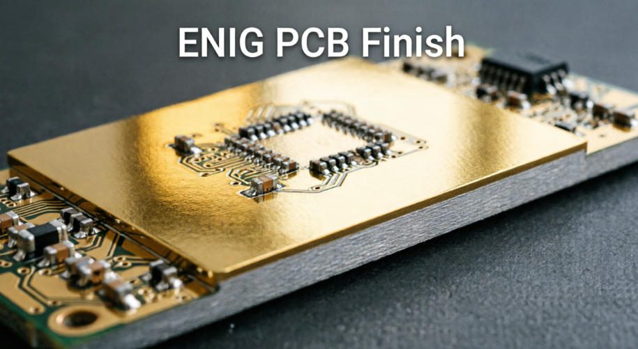
What Does ENIG Mean in PCB Manufacturing? (ENIG PCB Finish Explained)
ENIG (Electroless Nickel Immersion Gold) is a two‑layer metallic surface finish for PCBs, and it’s one of the most reliable options for modern ENIG PCB manufacturing. It coats exposed copper with a nickel layer (3–6 μm) followed by a thin gold layer (0.05–0.23 μm) via chemical deposition. ENIG delivers flatness, oxidation resistance, and reliable solder joints—key benefits that make ENIG for PCBs a top choice for high-performance electronics. This guide breaks down ENIG, its uses, pros and cons, and how it compares to other PCB surface finishes.
How Does the ENIG Process Work on PCBs? (Step-by-Step for ENIG PCB Manufacturing)
Unlike electrolytic plating, ENIG uses chemical deposition—no electric current is needed for ENIG PCB manufacturing. The process is straightforward but requires precise control to ensure quality results.
- Step 1: Pre‑treatment – Clean, micro-etch, and activate copper pads to ensure adhesion for the ENIG layers.
- Step 2: Electroless Nickel – Deposit a 3–6 μm nickel-phosphorus barrier to prevent copper diffusion into the solder.
- Step 3: Immersion Gold – Deposit 0.05–0.23 μm of gold to protect the nickel from oxidation before soldering.
- Step 4: Post‑treatment – Rinse and dry the PCB to ensure long-term protection for the ENIG finish.
What Are the Key Advantages of ENIG PCB Finish? (Why Choose ENIG for PCBs?)
ENIG outperforms many other PCB surface finishes, making ENIG for PCBs ideal for high-reliability designs across industries.
- Ultra‑flat surface – Perfect for 0.4mm pitch BGAs, QFNs, and HDI boards, a key benefit of the ENIG PCB finish.
- Long shelf life – 12–18 months of oxidation resistance, far longer than the 3–6 months offered by HASL.
- Excellent solderability – Gold dissolves quickly during reflow, creating strong nickel-solder bonds for reliable ENIG PCB.
- Low contact resistance – Stable performance for high-frequency circuits and gold-finger applications.
- RoHS compliant – Suitable for lead-free assembly, a must for modern ENIG PCB manufacturing.
What Are the Disadvantages and Risks of ENIG PCB Finish? (Challenges in ENIG Manufacturing)
While ENIG for PCBs is highly reliable, it has limitations that require careful management during ENIG PCB manufacturing.
- Higher cost – More expensive than HASL or OSP due to specialized materials and longer process time.
- Black pad risk – Nickel corrosion at the gold-nickel interface can weaken solder joints in ENIG PCB.
- Magnetic nickel layer – May affect ultra-high-speed signals (5G, PCIe 5.0) in ENIG PCB designs.
- Thin gold tolerance – Too thin a gold layer risks oxidation; too thick a gold layer increases brittleness in the ENIG PCB finish.
ENIG vs. HASL vs. OSP: Which PCB Surface Finish Is Best? (ENIG PCB Finish Comparison)
Choose ENIG for PCBs for precision and reliability; use alternatives for cost-sensitive designs. Below is a detailed comparison of ENIG vs. common alternatives.
| Feature | ENIG | HASL | OSP |
|---|---|---|---|
| Surface Flatness | Excellent (ideal for fine-pitch ENIG PCB) | Poor (uneven, not suitable for BGAs) | Good |
| Shelf Life | 12–18 months (ENIG PCB finish standard) | 3–6 months | 6–12 months |
| Solderability | Excellent | Good | Fair |
| Cost | High | Low | Very Low |
| Best For | BGA/QFN, HDI, high-reliability ENIG PCB | Through-hole, low-cost designs | Simple SMT, low-budget projects |
Which Industries Use ENIG PCBs Most? (ENIG PCB Finish Applications)
ENIG for PCBs is preferred for high-performance electronics across four key sectors, where reliability and precision are critical.
- Consumer Electronics – Smartphones, wearables, and laptops use ENIG PCB for fine-pitch components and high-density interconnects.
- Medical Electronics – Diagnostic equipment and implantable devices rely on the ENIG PCB finish for biocompatibility and reliability.
- Automotive Electronics – Engine control modules, ADAS, and EV battery boards need ENIG for PCBs for stability.
- Communication Infrastructure – 5G base stations and routers use ENIG PCB for low signal loss.
What Is the Typical Thickness of ENIG Layers in PCB Manufacturing? (ENIG PCB Specs)
Standard ENIG thickness balances performance, reliability, and cost for ENIG PCB manufacturing.
- Nickel (Ni): 3–6 μm – Acts as a robust diffusion barrier between copper and solder.
- Gold (Au): 0.05–0.23 μm – Protects nickel from oxidation during storage.
Thinner gold saves cost but reduces shelf life; thicker gold improves durability but raises the price of ENIG PCB.
How to Avoid Black Pad Defects in ENIG PCBs? (ENIG Manufacturing Tips)
Black pad (nickel corrosion) is a common risk in ENIG PCB manufacturing, but it can be prevented with proper process control.
- Control nickel phosphorus (7–9%) – Prevents excessive corrosion and brittleness in ENIG PCB.
- Maintain bath chemistry – Strict pH and temperature controls ensure consistent ENIG PCB finish.
- Limit gold immersion time – Minimize nickel attack during production.
- Use experienced manufacturers – Reduce black pad risk with strict quality control.
When Should You Choose ENIG Over Other PCB Surface Finishes? (ENIG for PCBs Use Cases)
Select ENIG for PCBs for designs requiring precision, reliability, or long storage.
- Fine‑pitch components (BGA, QFN, CSP) needing flat pads
- High‑density (HDI) boards with tight routing and small vias
- Long shelf life (6+ months) before assembly
- High‑frequency circuits needing stable, low-loss connections
- Gold finger or contact surfaces requiring durability
FAQ – Common Questions About ENIG PCB Finish (ENIG for PCBs)
Is ENIG the same as immersion gold in PCB manufacturing?
Yes, ENIG is often called immersion gold; ENIG specifically refers to the full nickel-gold stack used in ENIG PCB manufacturing.
Can ENIG PCBs be reflowed multiple times during assembly?
Yes, the ENIG PCB finish withstands 3+ lead-free reflow cycles with consistent quality.
Is ENIG suitable for flexible PCBs (FPC)?
Yes, electroless plating delivers uniform coverage on FPC surfaces, making ENIG PCB ideal for flexible designs.
Does ENIG affect signal integrity at high frequencies?
The nickel layer may impact extreme high frequencies; ENEPIG is recommended for applications above 100GHz.
What is the shelf life of ENIG PCBs?
ENIG PCB finish offers 12–18 months of shelf life in sealed, dry packaging.
Do ENIG PCBs require special handling during assembly?
No, but avoid touching gold pads to preserve solderability of your ENIG PCB.
ENIG PCB Design and Specification Best Practices
- Specify thickness clearly: Nickel 3–5 μm, gold 0.05–0.15 μm
- Follow IPC‑4552 standard for consistent ENIG PCB finish quality
- Avoid over‑specifying gold to control costs
- Request a DFM review to optimize manufacturability
Why Partner With Thindry for Your ENIG PCB Needs?
Thindry specializes in ENIG PCB manufacturing and delivers high-quality ENIG PCB with strict process control.
We offer customized solutions and free DFM reports to optimize your design for performance and reliability.
Whether you need prototypes or mass production, we ensure your ENIG PCB meets global industry standards.
Contact us at sales@pcbtry.com to discuss your project and place your order today.


0 Comments