
If you want to build a PCB at home, you can complete the entire process with basic tools and common materials. This detailed tutorial fully explains how to build a PCB at home through proven DIY workflows, covering design, fabrication, assembly, and functional testing. Suitable for electronics hobbyists and early-stage prototype developers, homemade PCB production shortens iteration cycles and lowers experimental barriers for small-scale circuit projects.
What Are the Best Methods to Build a PCB at Home?
Three mainstream practical methods support home PCB fabrication: toner transfer etching, photoresist UV etching, and desktop CNC milling. Toner transfer remains the most beginner-friendly and cost-effective option. Photoresist technology delivers finer trace accuracy for compact circuits. CNC milling offers a chemical-free, clean production solution for users who want to avoid corrosive liquids.
| Method | Overall Cost | Trace Precision | Operation Difficulty | Core Application Scenarios |
|---|---|---|---|---|
| Toner Transfer Etching | Low | Basic | Very Easy | Single-layer circuits, beginner projects, simple prototypes |
| Photoresist UV Etching | Medium | High | Moderate | Fine line traces, double-layer boards, high-precision prototypes |
| Desktop CNC Milling | Moderate-High | High | Moderate | Chemical-free processing, rapid dry fabrication, small batch trial runs |
Toner Transfer Method (Top Choice for Beginners)
Required supplies include a laser printer, heat-resistant glossy paper, household iron, copper-clad FR4 substrate, ferric chloride etchant, and fine-grit sandpaper.
This method supports a minimum trace width of 0.8mm, fully meeting the wiring needs of daily low-complexity electronic circuits.
Photoresist Etching Method (High Precision Upgrade)
Core tools consist of a UV exposure lamp, pre-coated photoresist copper board, mild developer solution, and professional etching liquid.
It achieves a minimum trace width of 0.4mm, ideal for dense component layout and miniaturized circuit design demands.
CNC Milling Method (Chemical-Free Safe Production)
A compact desktop CNC router, carbide micro drill bits, and standard copper-clad boards are the only necessities.
The mechanical cutting process eliminates chemical pollution risks and shortens post-processing cleaning time effectively.
How to Design Your PCB Before Building at Home?
Complete standardized schematic drawing and layout planning before physical production to avoid structural flaws and connection errors. Free open-source EDA software such as KiCad is widely recognized for home circuit design. Reasonable design rule settings directly improve the yield rate of homemade PCBs.
Draw and Verify the Complete Schematic
Mark all electronic components, power circuits, and signal connections clearly. Confirm component footprints and electrical logic to eliminate design defects in advance.
Complete Reasonable PCB Layout
Optimize component placement to reduce crossing traces and shorten signal transmission paths. Adding a complete ground plane effectively suppresses external electromagnetic interference for stable circuit operation.
Export High-Quality Printing Files
Output circuit layer files in high-resolution black and white format. Mirror the bottom copper layer to ensure accurate pattern transfer during subsequent heating and processing steps.
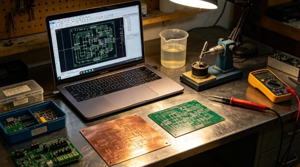
What Tools and Materials Do You Need for Home PCB Building?
Professional factory-level equipment is unnecessary for homemade PCB production. A complete set of daily tools and safe conventional materials can meet most personal prototype production needs. Protective equipment is essential to ensure operational safety during etching procedures.
Essential Hand Tools
- Black-and-white laser printer for pattern printing
- Constant-temperature iron or portable laminator
- Mini electric drill with micro drill bits ranging from 0.6mm to 1.2mm
- Fine-grit waterproof sandpaper and industrial isopropyl alcohol
- Digital multimeter for circuit continuity and voltage testing
Core Production Materials
- Standard FR4 copper-clad circuit boards with 1mm to 2mm thickness
- High-gloss transfer printing paper
- Safe industrial-grade etchant and surface cleaning solvent
- Anti-oxidation cleaning agents and auxiliary fixing accessories
Necessary Safety Protection Supplies
Nitrile anti-corrosion gloves, impact-resistant safety goggles, and local ventilation equipment are essential. Use dedicated plastic containers to store corrosive solutions and prevent accidental contact damage.
How to Transfer Your PCB Design to Copper at Home?
Toner heat transfer is the most widely adopted home PCB patterning technique. Clean substrate surfaces, sufficient toner coverage, and stable heating pressure are three key factors for perfect pattern transfer results.
Polish and Clean the Copper Substrate
Cut the copper-clad board to the required size first. Polish the copper surface evenly with fine sandpaper to remove oxide layers, then wipe thoroughly with isopropyl alcohol to eliminate oil stains and dust.
Print Mirrored Circuit Patterns
Print the mirrored circuit layout on glossy transfer paper with maximum toner density settings. Never use inkjet printers, as water-based ink cannot adhere stably to copper surfaces.
Complete Thermal Transfer Processing
Place the printed pattern side tightly against the copper layer. Heat with a household iron at a stable temperature between 180°C and 200°C for 3 to 5 minutes with continuous even pressure.
Separate Paper and Confirm Patterns
Let the board cool naturally to room temperature, then soak it in warm water to soften the paper fiber. Gently peel off the base paper to retain the complete toner protective pattern on the copper surface.
How to Etch a PCB at Home Safely and Effectively?
Etching removes exposed redundant copper materials and retains circuit traces covered by toner. Maintain a ventilated operating environment and shake the solution appropriately to ensure uniform etching effects and prevent local over-corrosion.
Ferric Chloride Etching (Mild and Stable)
Pour the diluted ferric chloride solution into a sealed plastic container. Immerse the processed circuit board with the pattern facing upward.
Gently shake the container every one to two minutes; the conventional etching cycle lasts 15 to 30 minutes at room temperature. Rinse the board with clean water immediately after all redundant copper dissolves.
Hydrogen Peroxide Mixed Etching (Efficient and Fast)
Prepare a mixed solution with a 2:1 ratio of 3% hydrogen peroxide and diluted hydrochloric acid. This formula accelerates the etching reaction significantly.
The overall processing time is shortened to 5 to 15 minutes. After completion, neutralize the board with a weak alkaline solution before thorough cleaning.
Post-Etching Surface Treatment
Remove residual toner with acetone solvent, then clean the entire board with isopropyl alcohol. Dry the circuit board naturally and inspect traces for breaks, short circuits, or incomplete corrosion.
How to Drill and Finish Your Homemade PCB?
Precise drilling determines the assembly accuracy of through-hole components. Standardized edge finishing avoids solder bridging and structural burrs that affect long-term use stability.
Standard Drilling Operation Tips
Fix the printed drill position guide on the board surface for accurate positioning. Use vertical drilling operations to prevent elliptical holes caused by angle deviation.
Mark hole positions with a sharp fine probe in advance to reduce bit slipping and pad damage.
Overall Board Finishing Steps
Polish the board edges smoothly to remove sharp burrs and cutting residues. Clean all processing dust with volatile cleaning fluid and fully dry the surface.
Applying a thin layer of soldering flux enhances subsequent component welding efficiency and connection stability.
How to Solder Components and Test Your DIY PCB?
Standard soldering specifications and step-by-step functional testing ensure homemade PCBs operate normally. Control soldering iron temperature reasonably and adopt segmented detection methods to avoid circuit burnout.
Practical Through-Hole Soldering Standards
Fix components in place by bending pin legs after insertion. Heat the bonding pad and component pin simultaneously before adding an appropriate amount of solder.
Qualified solder joints present a smooth conical shape; trim excess pins after all welding work is completed.
Multi-Stage Functional Testing Process
First, conduct a full continuity test to check for short circuits between power and ground loops. Perform visual inspection to screen for cold solder joints, tin bridges, and peeling pads.
Carry out low-voltage power-on testing first to verify overall circuit performance and avoid high-voltage damage to handmade circuits.
What Core Industries Use DIY-Friendly PCB Designs?
Lightweight homemade PCB prototypes support rapid research and development verification across four mainstream industries. Each field adopts targeted PCB types to solve common design bottlenecks and mass production pre-verification demands.
Consumer Electronics
Single-layer FR4 circuit boards are widely used in wearable devices, smart home sensors, and portable audio equipment. Custom homemade PCB prototypes accelerate small-function module testing and reduce early research costs.
Industrial Control & Automation
Double-layer PCBs with complete ground planes apply to motor drive modules, on-site sensor terminals, and mini PLC peripheral circuits. Optimized anti-interference designs adapt to complex factory electromagnetic environments.
Medical Electronics
Compact high-precision single and double-layer PCBs serve portable diagnostic equipment and household health monitoring devices. Miniaturized handmade prototypes help verify low-power and high-stability circuit solutions.
LED & Lighting Systems
Aluminum-based thermal conductive PCBs are the core choice for high-power LED driver circuits. Independent homemade board production assists in testing heat dissipation structures and constant-current driving schemes for lighting products.
What Are Common Mistakes When Building a PCB at Home?
Most failures in homemade PCB production stem from non-standard preprocessing and rushed operation steps. Summarizing frequent errors helps optimize production workflows and improve the overall qualified rate of self-made circuit boards.
Insufficient surface cleaning causes incomplete toner transfer, while excessive etching time leads to broken fine traces. Improper drilling angles damage bonding pads, and unregulated soldering operations easily trigger short-circuit faults.
FAQ: Common Questions About Building a PCB at Home
Can beginners build double-layer PCBs at home independently?
Yes. With photoresist UV etching technology and positioning auxiliary tools, beginners can complete double-layer PCB production. Accurate alignment between upper and lower layers is the key to successful fabrication.
What is the minimum feasible trace width for homemade PCB projects?
The toner transfer method stably supports 0.8mm trace width. Photoresist etching reaches 0.4mm, and CNC milling can maintain 0.5mm high-precision wiring for miniaturized designs.
What is the total time required to build a complete home PCB?
Circuit design takes 1 to 2 hours, pattern transfer and etching require 30 to 60 minutes, and drilling, soldering and testing take another 30 to 60 minutes. The complete cycle ranges from 2 to 4 hours for a single board.
Why is a laser printer mandatory for toner transfer production?
Laser printer toner forms a high-temperature fusion protective layer on copper surfaces. Water-based ink from inkjet printers cannot resist corrosion by etching liquid and will peel off easily during processing.
Are home PCB etching processes safe for long-term operation?
Yes, with complete protective equipment and standardized waste liquid disposal. All etching materials used in civilian DIY scenarios are low-corrosion formulas, ensuring personal safety with proper ventilation.
Is homemade PCB suitable for high-speed signal circuit design?
No. High-speed circuits require strict impedance control, multi-layer stacked structures, and professional material specifications, which cannot be achieved by conventional home production methods.
When Is Professional PCB Manufacturing Better Than DIY Production?
Homemade PCB solutions are perfect for learning, hobby projects, and small-batch prototype verification. Professional manufacturing services show obvious advantages in complex design, high stability requirements and formal project delivery scenarios.
Scenarios Suitable for Home PCB Building
Simple single or double-layer circuits, small-quantity trial production within 5 pieces, rapid function verification, and electronic technology learning and experimental projects.
Scenarios Suitable for Professional Custom PCB Manufacturing
Multi-layer boards with four or more layers, high-speed signal and radio frequency circuits, products with industrial compliance requirements, and formal mass production orders with stable quality standards.
Get Custom PCB Solutions – On-Demand Customization + Free DFM Report
Learning how to build a PCB at home is valuable for technical accumulation and small prototype testing. However, for formal project development, mass trial production and high-precision circuit demands, professional manufacturing delivers more stable performance and consistent quality.
Thindry provides reliable custom PCB and PCBA manufacturing services for global hardware designers and technical researchers. We support on-demand customization of various circuit board types for consumer electronics, industrial control, medical electronics, and LED lighting industries.
Our team offers a free DFM report for every design to optimize structural rationality and avoid manufacturing risks. If you need high-quality customized PCB products and professional technical support, feel free to contact our business team. Email: sales@pcbtry.com


0 Comments