
If you’re working with PCBs, HASL finish PCB is a staple in electronic manufacturing, and understanding how to leverage this finish correctly can make or break your board’s performance and cost-efficiency. HASL finish PCB remains one of the most widely used surface finishes for its practicality, but it’s critical to know its sweet spots, limitations, and how it stacks up against alternatives for your specific project. This guide breaks down every key detail—from core use cases to troubleshooting—to help you select, implement, and optimize HASL finish PCBs for any electronic application.
What Is a HASL Finish PCB, and How Does It Work?
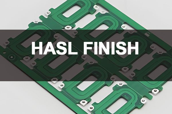
Core Definition of HASL PCB Finish
HASL, or Hot Air Solder Leveling, is a leaded or lead-free solder coating applied to bare PCB copper surfaces after manufacturing.
It melts solder and uses forced hot air to level the coating, creating a conductive, solderable layer for component attachment.
HASL finish PCB forms a protective barrier against copper oxidation, ensuring reliable soldering during assembly.
The Step-by-Step HASL Application Process
1. Clean the bare PCB to remove oil, dust, and oxidation from copper traces.
2. Immerse the board in a molten solder bath (lead-free Sn-Cu or Sn-Ag-Cu is standard today).
3. Use high-velocity hot air knives to wipe excess solder from the board’s surface and vias.
4. Cool the PCB rapidly to set the solder coating and ensure uniform leveling across all features.
Which Industries Benefit Most from HASL Finish PCB?
Automotive Electronics
HASL finish PCBs excel in automotive control modules and sensor boards.
The finish’s robust solderability works well for high-volume wave soldering, a staple in automotive manufacturing.
It resists vibration-induced solder joint failure in engine and chassis-mounted electronics.
Industrial Control & Automation
Industrial PLCs and motor drivers rely on HASL finish PCB for cost-effective mass production.
It tolerates the high-temperature operating environments of factory floor automation equipment.
It is ideal for through-hole component-heavy industrial boards with large copper pads.
Power & Power Electronics
Power supplies and inverters use HASL finish PCBs for their excellent electrical conductivity.
The thick solder layer handles high current loads without trace degradation.
It is compatible with the wave soldering processes used for power component assembly.
LED/Illumination
LED driver PCBs and lighting control boards leverage HASL finish PCB for low-cost scalability.
It works with the simple soldering requirements of LED surface-mount and through-hole components.
It resists minor environmental exposure in indoor and outdoor lighting fixtures.
What Are the Pros and Cons of HASL Finish PCB?
| Advantages of HASL Finish PCB | Disadvantages of HASL Finish PCB |
|---|---|
| Extremely cost-effective for high-volume PCB production | Uneven solder thickness on fine-pitch (<0.5mm) pads, causing bridging risks |
| Excellent solderability for all through-hole and most SMT components | Lead-free HASL has a higher melting point, increasing PCB thermal stress |
| Thick solder layer provides superior copper oxidation protection | Not ideal for HDI (High-Density Interconnect) PCBs with microvias |
| Compatible with standard wave and reflow soldering processes | Solder “tent” over vias can cause delamination in high-humidity environments |
| Well-established manufacturing process with global supplier availability | Poor planarity compared to ENIG or Immersion Silver, unsuitable for fine-pitch BGA |
| Easy to rework and repair solder joints on assembled boards | Lead-based HASL is restricted in RoHS-compliant electronic products |
How Does HASL Finish PCB Compare to Other PCB Surface Finishes?
| Feature | HASL Finish PCB | ENIG Finish PCB | Immersion Silver PCB | Immersion Tin PCB |
|---|---|---|---|---|
| Cost (per sq.in) | Lowest | Highest | Mid-Range | Mid-Range |
| Solderability | Excellent (long shelf life) | Excellent (unlimited shelf life) | Good (6–12 month shelf life) | Fair (3–6 month shelf life) |
| Fine-Pitch Compatibility | Poor (<0.5mm pads) | Excellent (0.2mm+ pads) | Good (0.3mm+ pads) | Good (0.3mm+ pads) |
| Planarity | Low (uneven surface) | High (ultra-smooth) | High (smooth) | High (smooth) |
| RoHS Compliance | Lead-free option available | 100% RoHS compliant | 100% RoHS compliant | 100% RoHS compliant |
| Environmental Resistance | Fair (susceptible to humidity) | Excellent (corrosion-resistant) | Fair (tarnishes easily) | Poor (prone to tin whiskers) |
| Ideal For | High-volume, through-hole, low-density PCBs | HDI, fine-pitch BGA, high-reliability PCBs | Mid-volume, mixed-technology PCBs | Short-run, low-humidity application PCBs |
| Rework Ease | Very Easy | Difficult (nickel corrosion risk) | Easy | Moderate (tin flaking risk) |
How to Optimize HASL Finish PCB for Maximum Performance?
Choose the Right HASL Formulation
Opt for lead-free Sn-Ag-Cu (SAC) HASL for RoHS compliance in consumer and industrial electronics.
Leaded HASL is still viable for non-RoHS aerospace or legacy equipment (per industry regulations).
Avoid low-quality solder alloys—they cause poor leveling and weak solder joints.
Design PCBs for HASL Compatibility
Keep pad pitch above 0.5mm to eliminate solder bridging risks on SMT components.
Enlarge via sizes (≥0.3mm) to ensure proper hot air leveling and prevent via plugging.
Add solder dams around sensitive components to block excess solder flow during application.
Control Manufacturing Process Parameters
Maintain solder bath temperature at 250–260°C (lead-free) to avoid PCB warpage.
Set hot air knife pressure to 30–50 PSI for uniform solder removal across the board.
Ensure post-HASL cleaning to remove flux residue, which causes long-term corrosion.
Store HASL Finish PCBs Correctly
Keep HASL finish PCB in sealed, dry packaging (≤30% humidity) at 18–25°C.
Avoid exposure to direct sunlight and industrial fumes, which accelerate oxidation.
Use PCBs within 6 months of manufacturing for optimal solderability (lead-free HASL).
What Common Issues Arise with HASL Finish PCB, and How to Fix Them?
Solder Bridging on Fine-Pitch Pads
Bridging occurs when hot air fails to remove excess solder between narrow pads.
Fix: Widen pad pitch to ≥0.5mm or use a finer hot air knife nozzle for precision leveling.
Manually debridge with a soldering iron and desoldering braid for small production runs.
Uneven Solder Thickness Across the PCB
Caused by inconsistent hot air pressure or uneven PCB immersion in the solder bath.
Fix: Calibrate air knives weekly and ensure the PCB is fully level during immersion.
Use a solder thickness gauge to inspect boards and reject units with >20% thickness variation.
Via Plugging or Partial Tenting
Excess solder flows into vias and hardens, blocking component pin insertion.
Fix: Increase hot air pressure or reduce PCB dwell time in the solder bath.
Design vias with solder masks to prevent solder penetration (mask-defined vias).
Copper Oxidation Under HASL Coating
Oxidation forms if the PCB is not cleaned properly before solder application.
Fix: Implement a multi-step cleaning process (alkaline wash → rinse → acid dip → rinse).
Inspect copper surfaces for oxidation pre-HASL with a magnifying glass or microscope.
PCB Warpage After HASL Application
Caused by excessive solder bath temperature or rapid cooling of the board.
Fix: Lower bath temperature to the minimum viable level (250°C for lead-free SAC).
Use a gradual cooling process (100°C → 50°C → room temp) to reduce thermal stress.
Add stiffeners to large PCBs (>200x200mm) to prevent warpage during manufacturing.
FAQ: Your Most Pressing HASL Finish PCB Questions Answered
Q: Is HASL finish PCB RoHS compliant for global electronic markets?
A: Yes, lead-free HASL (Sn-Ag-Cu or Sn-Cu alloys) is 100% RoHS compliant and accepted in all global markets, including the EU, US, and Asia. Leaded HASL is restricted for most consumer and industrial electronics but is allowed for specific aerospace and military applications with regulatory exemptions. HASL finish PCB with lead-free solder is the standard for commercial electronic production today.
Q: Can HASL finish PCB be used for HDI or fine-pitch BGA components?
A: No, HASL finish PCB is not recommended for HDI PCBs or fine-pitch BGA (<0.5mm pitch) components. The hot air leveling process creates an uneven solder surface, which causes poor contact and solder joint failure with fine-pitch components. ENIG is the preferred finish for HDI and BGA applications due to its ultra-smooth, planar surface.
Q: What is the shelf life of an unassembled HASL finish PCB?
A: Unassembled lead-free HASL finish PCB has a shelf life of 6–12 months when stored in sealed, dry packaging (≤30% humidity, 18–25°C). Leaded HASL PCBs have a longer shelf life (12–24 months) due to the more stable solder alloy. Oxidation of the solder coating will reduce solderability over time, so it’s critical to use PCBs within the recommended shelf life.
Q: Can HASL finish PCB be reworked after component assembly?
A: Yes, HASL finish PCB is one of the easiest finishes to rework. The thick solder layer allows for repeated soldering and desoldering of components without damaging the copper traces or pad surface. Use standard rework tools (soldering iron, hot air rework station) and avoid excessive heat (≥300°C) to prevent PCB delamination during rework.
Q: Is HASL finish PCB suitable for high-humidity or outdoor electronic applications?
A: Fair, but additional protection is recommended. HASL finish PCB is susceptible to humidity-induced corrosion and solder joint degradation in outdoor or high-humidity (>60% RH) environments. For these applications, apply a conformal coating (urethane or acrylic) to the assembled PCB to seal the HASL finish and protect against moisture, dust, and chemicals.
Q: How does the cost of HASL finish PCB compare to ENIG for high-volume production?
A: HASL finish PCB is 50–70% less expensive than ENIG for high-volume production (10,000+ units). HASL uses a simpler manufacturing process with lower raw material costs, making it the most cost-effective surface finish for large production runs. ENIG’s higher cost is due to its complex electroless plating process and precious metal (gold) raw materials.
When Should You Avoid Using HASL Finish PCB?
Fine-Pitch or HDI PCB Designs
Any PCB with pad pitch <0.5mm or microvias (HDI) should skip HASL—uneven solder causes bridging and poor component fit.
ENIG or Immersion Silver are far better choices for these high-density designs.
High-Reliability Aerospace/Avionics
Aerospace PCBs require ultra-consistent solder joints and environmental resistance.
HASL’s poor planarity and humidity susceptibility make it unsuitable; ENIG is the industry standard here.
Medical Electronic Devices
Medical PCBs (e.g., diagnostic equipment, implantable devices) need RoHS compliance and zero-failure reliability.
HASL’s thermal stress risk and uneven surface make ENIG the preferred finish for medical applications.
Consumer Electronics with Miniaturized Components
Smartphones, wearables, and tablets use fine-pitch BGA and micro-SMT components.
HASL finish PCB cannot support these miniaturized designs—ENIG or Immersion Tin is required.
How to Select a Reliable HASL Finish PCB Manufacturer?
Verify Manufacturing Certifications
Choose a manufacturer with ISO 9001 (quality) and IPC-A-600 (PCB standards) certifications.
For RoHS compliance, confirm the supplier uses lead-free SAC solder for HASL finish PCB.
Inspect In-Process Quality Control
Ask for process documentation—including solder bath calibration and hot air knife testing records.
Request sample PCBs to check for uniform solder thickness and no bridging/plugging.
Evaluate Industry Experience
Prioritize manufacturers with 5+ years of experience producing HASL finish PCB for your target industry.
Suppliers with automotive/industrial electronics experience understand strict performance requirements.
Check Lead Times and Scalability
Ensure the manufacturer can meet your high-volume lead times (typically 5–10 business days for HASL PCBs).
Confirm they can scale production up/down to match your project’s volume needs.
What Testing Is Required for HASL Finish PCB Before Assembly?
Solder Thickness Measurement
Use a digital thickness gauge to verify solder coating is 10–25μm (lead-free) across all pads/traces.
Reject boards with thickness variation >20% to avoid soldering issues.
Solderability Testing
Perform a wetting balance test to confirm the HASL finish solder wets copper pads quickly (≤2 seconds).
Poor wetting indicates oxidation and means the PCB is unfit for assembly.
Visual and Microscopic Inspection
Inspect PCBs for bridging, via plugging, and uneven leveling with a 20x magnifying glass.
Use a microscope to check for flux residue and copper oxidation under the solder layer.
Warpage Testing
Measure board flatness with a straight edge—reject HASL finish PCB with warpage >0.75% of total board size.
Warped boards cause component misalignment during assembly.
How to Integrate HASL Finish PCB into Your Supply Chain?
Align with PCB Assembly Partners
Confirm your contract manufacturer (CM) has wave soldering capabilities for HASL finish PCB.
Share your PCB design files with the CM to optimize soldering parameters for your board.
Set Clear Quality Specifications
Include HASL finish requirements (alloy type, solder thickness, RoHS) in your PCB purchase order.
Define acceptance/rejection criteria for testing to avoid quality disputes with suppliers.
Optimize Inventory Management
Order HASL finish PCB in batches that match your assembly schedule to avoid shelf life expiration.
Store PCBs in sealed packaging with desiccant packs to maintain solderability.
Establish a Supplier Qualification Process
Audit new HASL PCB suppliers annually to verify process consistency and quality.
Maintain a list of 2–3 qualified suppliers to avoid production delays from supply chain issues.
What Future Trends Impact HASL Finish PCB Use in Electronics?
Shift to Miniaturization and HDI
The growth of miniaturized consumer and industrial electronics is reducing HASL’s market share for fine-pitch designs.
HASL finish PCB will remain dominant for low-density, high-volume through-hole PCBs, however.
Advancements in Lead-Free HASL Alloys
New lead-free solder alloys (e.g., Sn-Ag-Cu-Bi) are being developed to lower melting points and reduce PCB thermal stress.
These alloys will make HASL finish PCB more compatible with heat-sensitive PCB materials (e.g., flex PCBs).
Increased Focus on Sustainability
Electronics manufacturers are demanding more eco-friendly PCB processes—HASL suppliers are optimizing waste reduction and energy use.
Recyclable solder alloys for HASL are in development to align with circular economy goals in the electronics industry.
Hybrid Surface Finishes
Many manufacturers are combining HASL finish PCB with ENIG on the same board (HASL for through-hole, ENIG for fine-pitch SMT).
This hybrid approach balances cost-efficiency and performance for mixed-technology PCB designs.
At Thindry, we specialize in high-quality HASL finish PCB production for automotive electronics, industrial control, power electronics, and LED/illumination applications. Our lead-free HASL PCBs are RoHS compliant, manufactured to IPC standards, and optimized for high-volume production and reliable soldering. Whether you need standard HASL finish PCBs or custom designs tailored to your project’s unique requirements, our team of engineering experts will deliver precision and consistency with fast lead times. For all your HASL finish PCB needs, place your order by emailing our sales team at sales@pcbtry.com—we’re ready to support your electronic manufacturing projects with top-tier PCB solutions.


0 Comments