
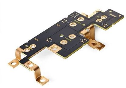
When seeking a reliable manufacturer for Heavy Copper PCB Prototype, Thindry is your top choice. We specialize in high-precision Heavy Copper PCB Prototype fabrication for high-power, harsh-environment applications, delivering consistent quality that meets strict industry standards. Whether your project involves medical devices, aerospace systems, or industrial equipment, our engineering team ensures your prototype aligns with performance and reliability requirements.
Thindry stands out for our expertise in overcoming heavy copper PCB manufacturing challenges. We hold ISO 9001:2015 certification, master advanced etching and lamination technologies, and offer 24/48h sample turnaround. Our tailored solutions for 2oz to 20oz copper thicknesses, combined with rigorous quality control, make us the trusted partner for complex prototype projects.
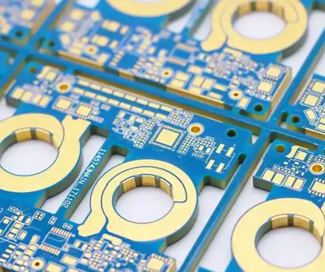
Heavy Copper PCB Prototype
What Is a Heavy Copper PCB Prototype?
A Heavy Copper PCB Prototype is a test version of a printed circuit board with copper layers thicker than standard PCBs. While standard PCBs use 1oz (35μm) copper, heavy copper prototypes range from 2oz (70μm) to 20oz (700μm) per square foot, with extreme designs exceeding this range. These prototypes are engineered to validate high-current handling, heat dissipation, and mechanical robustness for power-intensive applications.
Key Characteristics of Heavy Copper PCB Prototypes
- Superior current capacity: Thicker copper enables higher amperage without overheating or trace damage.
- Enhanced heat dissipation: Reduces hotspots and extends component lifespan in high-power circuits.
- Strong mechanical strength: Resists vibration, thermal cycling, and supports heavy components.
What Copper Thickness Is Right for Heavy Copper PCB Prototypes?
The ideal copper thickness for your Heavy Copper PCB Prototype depends on current requirements, thermal performance, and mechanical needs. Below is a breakdown of common thicknesses and their applications to guide your prototype design.
| Copper Thickness (oz/ft²) | Physical Thickness (μm) | Typical Prototype Applications |
|---|---|---|
| 2oz | 70 | Entry-level power supplies, basic motor controllers |
| 3-6oz | 105-210 | Industrial power electronics, medical devices (defibrillators) |
| 8-20oz | 280-700 | Aerospace systems, high-power inverters, welding equipment |
How to Overcome Heavy Copper PCB Prototype Manufacturing Challenges?
Manufacturing Heavy Copper PCB Prototypes poses unique challenges due to thick copper’s rigidity and etching complexity. Here are proven solutions for key bottlenecks to ensure prototype quality.
Lamination Process Challenges & Fixes
Thick copper causes uneven pressure distribution and resin filling issues. Pre-treat copper foil (roughening + passivation) to boost resin adhesion, use high-flow resin (30% flowability), and apply stepwise pressure during lamination. This reduces delamination rate to ≤1.5% and maintains flatness.
Etching Precision Solutions
Use acidic copper chloride etching solution (70g/L Cu²+ concentration) with etching accelerators. Adjust time based on thickness (4oz = 120 seconds) and add 0.03mm design compensation to keep line width deviation ≤±0.01mm. Plasma cleaning removes burrs for clean edges.
What Industries Rely on Heavy Copper PCB Prototypes?
Heavy Copper PCB Prototypes are critical for industries demanding high reliability and performance. Below are real-world applications showcasing their value.
Medical Industry
We developed a 4oz heavy copper prototype for a portable defibrillator. The thick copper layers ensured stable 200A current delivery and efficient heat dissipation, meeting ISO 13485 standards for medical device safety.
Aerospace Industry
Our 10oz prototype for an aircraft power distribution unit withstood extreme temperature cycles (-55℃ to 125℃) and vibration, validating its suitability for harsh aerospace environments.
Industrial Equipment
A 6oz prototype for a industrial welding machine supported 150A continuous current, reducing component failure rate by 40% compared to standard PCB designs.
How Does Heavy Copper PCB Prototype Compare to Standard PCB Prototype?
The choice between Heavy Copper PCB Prototype and standard prototype depends on application demands. The table below highlights core differences to inform your selection.
| Feature | Heavy Copper PCB Prototype | Standard PCB Prototype |
|---|---|---|
| Copper Thickness | 2-20oz/ft² | 0.5-3oz/ft² |
| Current Capacity | High (tens to hundreds of amps) | Low to moderate (up to 10 amps) |
| Heat Dissipation | Excellent | Basic (relies on environment) |
| Ideal Applications | Power electronics, aerospace, medical | Consumer electronics, low-power devices |
FAQ: Common Heavy Copper PCB Prototype Questions
Can Heavy Copper PCB Prototypes Be Used in High-Temperature Environments?
Yes. Heavy Copper PCB Prototypes excel in high-temperature environments. Thicker copper layers have lower thermal resistance, spreading heat efficiently to prevent component overheating. They are widely used in automotive engine bays and industrial furnaces with operating temps up to 150℃.
How Long Does It Take to Fabricate a Heavy Copper PCB Prototype?
Turnaround time varies by copper thickness and complexity, but Thindry offers 24/48h sample delivery for most 2-6oz Heavy Copper PCB Prototypes. Extreme 8-20oz prototypes take 3-5 days due to specialized processing steps like gradient lamination and precision etching.
What Design Rules Apply to Heavy Copper PCB Prototypes?
Adjust trace width based on copper thickness (e.g., 4oz copper needs 0.8mm width for 30A current). Add etching compensation (0.02-0.03mm) to maintain dimensional accuracy. Use larger vias (≥0.4mm) to ensure reliable connections with thick copper layers.
Are Heavy Copper PCB Prototypes Compatible with SMT Components?
Yes. Proper process control ensures Heavy Copper PCB Prototypes work with SMT components. We use specialized solder paste and reflow profiles to accommodate thick copper’s thermal mass, ensuring strong solder joints without component damage.
How to Ensure Quality for Heavy Copper PCB Prototypes?
Implement rigorous inspection: AOI (Automated Optical Inspection) for etching defects, X-ray for via quality, and thermal cycling tests (-40℃ to 85℃, 1000 cycles) to validate reliability. Thindry’s ISO-certified process ensures 92%+ prototype first-pass yield.
What Are the Design Tips for Heavy Copper PCB Prototypes?
Optimize your Heavy Copper PCB Prototype design with these actionable tips to enhance performance and manufacturability.
- Balance power and control circuits: Integrate both on one board to reduce size and improve reliability.
- Use thermal vias: Place vias near high-power components to boost heat transfer to the opposite layer.
- Choose the right substrate: FR-4 works for most applications; select high-Tg FR-4 (Tg≥170℃) for extreme temps.
How to Validate Heavy Copper PCB Prototype Performance?
Performance validation ensures your Heavy Copper PCB Prototype meets design specs. Conduct these key tests:
Electrical Testing
Measure current-carrying capacity and impedance using TDR (Time Domain Reflectometry) to confirm signal integrity. Test for short circuits and continuity across all traces.
Thermal Testing
Use infrared thermography to map hotspots under maximum load. Ensure no area exceeds the component’s rated temperature (typically 85℃ for industrial parts).
Mechanical Testing
Perform vibration and thermal cycling tests to simulate real-world conditions. Check for solder joint cracks and trace damage post-testing.
What Certifications Matter for Heavy Copper PCB Prototypes?
Certifications validate the quality and reliability of Heavy Copper PCB Prototypes, especially for regulated industries. Prioritize manufacturers with these certifications:
- ISO 9001:2015: Ensures consistent manufacturing processes.
- ISO 13485: Mandatory for medical device prototypes.
- IPC-A-600: Standards for PCB acceptability and quality.
How to Reduce Warpage in Heavy Copper PCB Prototypes?
Warpage is a common issue with Heavy Copper PCB Prototypes due to uneven thermal expansion. Mitigate it by using symmetric layer stacks, optimizing lamination temperature curves (1℃/min heating/cooling), and selecting low-CTE (Coefficient of Thermal Expansion) substrates.
What Are the Advantages of Custom Heavy Copper PCB Prototypes?
Custom Heavy Copper PCB Prototypes are tailored to your project’s unique needs, offering advantages over off-the-shelf options. They optimize copper thickness, trace layout, and substrate selection for maximum performance, reducing redesign costs and accelerating time-to-market.
How to Choose a Heavy Copper PCB Prototype Manufacturer?
Select a manufacturer with expertise in heavy copper processing, proven industry experience, and strict quality control. Prioritize those offering fast turnaround, custom solutions, and certification compliance to ensure your prototype meets requirements.
Thindry provides high-quality Heavy Copper PCB Prototype fabrication with 2oz to 20oz copper thickness options, 24/48h sample delivery, and ISO-certified processes. Our engineering team supports medical, aerospace, and industrial projects with tailored solutions. For your next prototype project, contact us at sales@pcbtry.com to place an order.


0 Comments