
AI servers and high-speed network systems depend on high-density, high-power components such as GPUs, FPGAs, ASICs, and CPUs — most of which come in complex BGA packages. These chips require stable, low-loss, high-frequency connections, and that’s where advanced HDI PCBs come into play.
At Thindry Circuit, we specialize in one-stop manufacturing and assembly of AI server PCB like HDI and high-speed PCBs for AI servers, switches, routers, and data center interface cards. Our boards are engineered to handle gigabit-level data transmission, offering superior signal integrity, power distribution, and heat management.
What is AI Server PCB?
An AI server PCB (Printed Circuit Board) is a high-performance, high-layer, high-speed circuit board designed specifically for servers that run artificial intelligence workloads such as machine learning training, inference, and large-scale data processing.
Unlike standard server PCBs, an AI server PCB must support extreme data bandwidth, massive power delivery, and advanced thermal management to handle GPUs, AI accelerators, and high-speed interconnects reliably.
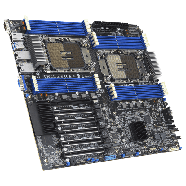
AI Server PCB
Why AI Server PCB Always Use High-Speed or HDI PCB?
AI servers process an enormous amount of data in real time. The boards inside must handle complex signal paths between CPUs, GPUs, and memory modules with zero delay or distortion. Traditional PCBs can’t manage such requirements due to limited routing density and slower signal propagation.
High-Density Interconnect (HDI) PCBs solve these challenges by incorporating microvias, buried vias, and fine-line routing. This structure allows more signal layers and components to fit into compact areas, reducing electrical noise and latency.
Moreover, high-speed PCB design minimizes signal loss across long trace lengths. AI servers often operate with multi-gigabit communication interfaces like PCIe Gen5, DDR5, or 400G Ethernet — all demanding stable impedance and low dielectric loss. Without HDI or high-speed structures, data synchronization would fail, leading to unstable system performance.
AI Server PCB vs Conventional PCB
| Feature | AI Server PCB | Conventional PCB |
| Layer Count | 10–24 layers or more | Typically 4–8 layers |
| Type | HDI or hybrid multilayer | Standard multilayer |
| Signal Speed | Multi-Gbps (PCIe Gen5, DDR5, 400G Ethernet) | Low to medium speed |
| Dielectric Material | Low-loss laminate (Rogers, Megtron, Isola) | FR-4 |
| Thermal Control | Copper coin, thermal vias, metal core | Standard copper plane |
| Via Structure | Microvias, buried vias, blind vias | Through-hole vias only |
| Power Requirement | High current, low voltage | Moderate current |
| Application | AI servers, data centers, network cores | Consumer or industrial electronics |
AI server PCBs are purpose-built for signal integrity, density, and reliability. Conventional PCBs, though cost-effective, it cannot meet the stringent demands of high-frequency AI computing.
Materials Used in AI Server PCB
| Material Type | Example | Key Properties | Application Layer |
| Low-Loss Laminate | Rogers 4003C / Megtron 6 | Stable Dk, low Df | High-speed signal layers |
| Hybrid Stackup | Megtron + FR-4 | Cost-efficient with high-frequency stability | Mixed digital and power layers |
| High-Tg FR-4 | Tg > 170°C | Better thermal endurance | Core or power planes |
| Prepreg with High Thermal Conductivity | Panasonic R-5775 | Heat spreading between layers | Thermal management regions |
| Surface Finish | ENIG / ENEPIG | Excellent solderability, wire bonding reliability | Component pads and fine-pitch BGAs |
| Copper Foil | 1oz–3oz | Improved current capacity and thermal spreading | Power delivery planes |
Key Parts in AI Server PCB
AI server PCBs integrate multiple critical sections that collectively sustain performance and reliability:
- CPU & GPU Zone: Hosts high-power processors with thermal vias and copper pads for efficient heat transfer.
- Memory Interface: DDR4/DDR5 channels requiring impedance control and matched trace lengths.
- High-Speed I/O Area: PCIe, NVLink, and Ethernet ports with tight routing and shielding.
- Power Distribution Network (PDN): Multi-layer copper planes delivering stable power to every core.
- Clock & Control Section: Synchronizes timing across chips, essential for coordinated AI computation.
- Cooling Integration Area: Embedded thermal vias or copper coins under BGA packages to handle up to 300W per chip.
Considerations When Designing AI Server PCB
Designing an AI server PCB is far more complex than developing a conventional board. These systems operate at extremely high data rates and handle large power flows for processors like GPUs, FPGAs, and custom AI accelerators. Each design stage—stackup, routing, power delivery, and thermal management—directly affects the final computing performance. Below are key considerations engineers must account for, supported by relevant data and best practices.
1. Signal Integrity (SI) and High-Speed Routing
AI servers process data at speeds often exceeding 56–112 Gbps per channel in PCIe Gen 5 and 400G Ethernet interfaces. At such frequencies, even a 0.1 mm variation in trace width or spacing can cause impedance mismatch, resulting in data loss or timing jitter.
Designers must:
- Maintain differential impedance at 85 Ω ± 5% for PCIe and 100 Ω ± 5% for Ethernet channels.
- Keep trace length skew below 5 mils for matched pairs to prevent phase delay.
- Use low-loss dielectric materials (Dk ≈ 3.2–3.5, Df ≤ 0.004) to minimize insertion loss.
High-speed signal layers are often positioned in the middle of the stackup, sandwiched between solid reference planes, ensuring low electromagnetic interference (EMI) and signal isolation.
2. Power Delivery Network (PDN) Design
AI processors like NVIDIA’s A100 or AMD MI300 demand more than 300 A at core voltages below 1 V. Supplying such massive current uniformly requires a low-inductance PDN.
Design guidelines include:
- Using 1–3 oz copper planes for primary power layers.
- Placing multiple parallel vias near BGA pads to reduce current bottlenecks.
- Decoupling capacitors arranged in an L-C-L topology, with ultra-low ESR types close to the chip.
- Maintaining plane impedance below 100 mΩ from DC up to 100 MHz for stable transient response.
PDN simulation tools like Ansys SIwave or Keysight ADS are often used to verify power ripple and impedance distribution before fabrication.
3. Thermal Management
AI workloads run continuously, generating significant heat. For example, an AI accelerator may reach 250–300 W thermal design power (TDP). PCB designers must build efficient heat pathways:
- Embed copper coins directly under the GPU or FPGA to conduct heat to the heatsink.
- Insert thermal vias (0.3 mm Ø, 1.0 mm pitch) under BGA arrays to enhance conduction.
- Use prepregs with thermal conductivity ≥ 1.0 W/m·K to improve layer-to-layer heat spreading.
For critical zones, integrate aluminum or copper base plates into the board stackup.
4. Layer Stackup Optimization
AI server PCBs typically range from 14 to 24 layers, combining signal, ground, and power planes.
A well-structured example might be:
- Signal layers: 8–10
- Power/Ground planes: 6–8
- Control & low-speed layers: 2–4
Stack symmetry (copper balance ± 10%) is vital to prevent warpage during lamination. Controlled dielectric thicknesses of 0.1–0.2 mm are common between high-speed layers to maintain consistent impedance.
5. EMC/EMI Control
AI server environments are dense with switching regulators and clock sources. Shielding techniques include:
- Adding guard traces or ground stitching vias between sensitive nets.
- Ensuring continuous ground planes under high-speed lines.
- Maintaining return path continuity for all differential pairs.
EMI testing often targets Class A (industrial) compliance per CISPR 32 standards.
Why Choose Thindry Circuit for AI Server PCB Manufacturing?
At Thindry Circuit, we combine advanced engineering, precision manufacturing, and strict quality control to produce PCBs that meet the challenges of AI computing.
We are certified with ISO9001, ISO13485, and we use a MES traceability system to monitor every stage of production. Our team provides DFM consultation, stackup optimization, and thermal simulation support to ensure the design performs flawlessly.
Whether it’s a 24-layer AI server mainboard or a compact high-speed data card, we deliver consistent performance, short lead times, and cost-effective solutions for global customers.
Our AI Server PCB Cases
Case 1: AI Computing Board for FPGA Acceleration
- [1] Chip: Xilinx XCKU060 FPGA (1156 pins, 0.8 mm pitch)
- [2] Maximum Current: 20 A (core supply)
- [3] Memory Interface: Four DDR4 channels @ 2400 MHz
- [4] PCB Layers: 20 layers
- [5] Material: Isola I-Tera MT40 (low Df 0.0031 @ 10 GHz)
- [6] Surface Finish: ENEPIG (1 µin Pd / 4 µin Au)
- [7] Features: HDI stackup with 1+N+1 microvias, impedance control ±5%, copper coin under FPGA, thermal via matrix, and back-drilled via stubs for high-speed IO.
This board powers an AI inference module used in edge-server systems. It supports up to 120 Gbps data transfer and stable operation under ambient temperatures up to 90 °C.
Case 2: GPU Server Mainboard for Data Center Application
- [1] Chip: NVIDIA A100 GPU module and dual AMD EPYC processors
- [2] Maximum Current: 280 A (total system)
- [3] Memory Interface: Eight DDR5 channels @ 5600 MT/s
- [4] PCB Layers: 22 layers (hybrid HDI design)
- [5] Material: Panasonic Megtron 7 + FR-4 Hybrid (Dk 3.2, Df 0.002 @ 10 GHz)
- [6] Surface Finish: ENIG (2 µin Au / 4 µin Ni)
- [7] Features: Controlled impedance for PCIe Gen 5 (112 Gbps), embedded copper coins for thermal transfer, dual power backplanes, and vacuum lamination to prevent voids.
The mainboard serves as the backbone of a data-center AI training rack, sustaining continuous high-load computation 24/7 with excellent power stability and signal performance.
When you need precision, reliability, and speed in your AI server PCB — Thindry Circuit is your trusted partner.


0 Comments