
PCB and PWB are two frequently used technical terms in the electronics manufacturing industry. PWB stands for Printed Wiring Board, while PCB is short for Printed Circuit Board. Both are indispensable basic components in modern electronic products, playing a crucial role in connecting, fixing, and supporting electronic components.
In practical applications, PCB and PWB are often used interchangeably, but they still differ significantly in terms of design complexity, manufacturing processes, and applicable scenarios. This article will systematically introduce the definitions, structural characteristics, and manufacturing methods of PCB and PWB. It will also analyze their main application areas and key selection points to help make more efficient and accurate decisions in electronic design and manufacturing.
What is a printed circuit board (PWB)?
PWB (Printed Waveform Board) creates stable current paths by printing or etching conductive traces on a non-conductive substrate, enabling various electronic components to transmit signals and coordinate functions.
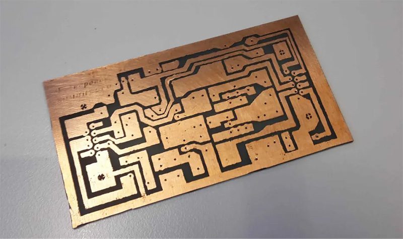
In the early stages of electronic technology development, PWB functions were relatively simple, typically not containing embedded components, serving only as a physical carrier for component mounting and interconnection. Their structure was mostly a single-sided board, with conductive traces distributed only on one side of the substrate. This limited circuit complexity to some extent, making them more suitable for electronic devices with simple structures and clearly defined functions.
The substrate material is a key factor affecting the performance and reliability of PWB. Common materials include phenolic paper, epoxy glass, and polyimide. Phenolic paper is low-cost and suitable for basic applications; epoxy glass has better electrical insulation and mechanical strength, suitable for demanding industrial applications; while polyimide, with its excellent high-temperature resistance and chemical resistance, is widely used in harsh environments such as aerospace and military.
What is a printed circuit board (PCB)?
Compared to earlier PWB (Power-Waveboard) designs, PCB (Printed Circuit Boards) significantly improve design flexibility and component integration density by introducing multi-layer conductive structures and insulating media, better meeting the application requirements of complex circuits and high-speed signals.
PCB conductive traces are typically made of copper, which, due to its excellent conductivity, good thermal stability, and mature manufacturing process compatibility, has become the industry standard choice. Based on application complexity and performance requirements, PCB can be categorized into single-sided, double-sided, and multi-layer structures:
Single-sided PCB have a simple structure and are suitable for basic electronic products;
Double-sided PCB improve routing flexibility through double-layer traces;
Multi-layer PCB achieve high-density design and better signal integrity through multi-layer interconnects, and are widely used in high-performance electronic devices.
PCB serve as a stable carrier for electronic components (such as resistors, capacitors, diodes, transistors, integrated circuits, and connectors). Their high reliability and strong adaptability make them widely used in consumer electronics, industrial control, communication equipment, and high-end fields such as aerospace and military.
Differences between PCB and PWB components and materials
Printed circuit boards (PWB) and printed circuit boards (PCB) differ significantly in their components and materials. The basic components of a PWB include a substrate, conductive traces, and vias (or through-holes). The substrate is typically made of a non-conductive material, providing mechanical support and electrical insulation for the traces. Common materials include phenolic paper, epoxy fiberglass prepreg, and polyimide, each differing in performance and cost. Conductive traces are generally made of copper, with thickness determined by current-carrying capacity requirements. Through-holes or plated through-holes (PTH) are used to connect traces on different layers or provide component mounting points. PWB are usually single-sided designs, suitable for simple circuits and basic electronic devices.
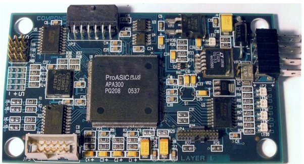
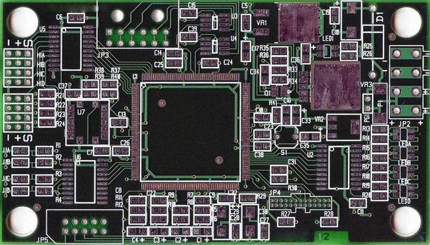
In contrast, PCB are an upgrade from PWB, suitable for complex circuit designs. The main components of a PCB include a substrate, conductive traces, vias, and solder mask. For the substrate, FR-4 material is commonly used, but high-performance polyimide or Rogers materials can also be selected to meet high-frequency or high-temperature environment requirements. Conductive traces are still primarily copper, with thickness and number of layers adjustable according to current and design complexity. Via types are more diverse, including through-hole, blind, and buried vias, used for interlayer connections and component mounting, respectively. Solder mask covers the PCB surface to prevent oxidation, short circuits, and solder bridging. Common materials include liquid crystal imaging (LPI), dry film, or screen-printed solder mask to meet different resolution and cost requirements.
PWB is more suitable for simple circuits, while PCB supports multilayer, high-density, and high-performance applications, offering superior electrical performance, reliability, and manufacturing flexibility.
Design differences between PCB and PWB
The core difference between PCB and PWB at the design level lies in circuit complexity and integration capabilities. PWB are typically single-sided structures, with conductive traces distributed only on one side of the substrate. This limited space makes them more suitable for electronic products with simple functions and a small number of components.
In contrast, PCB support single-sided, double-sided, and multi-layer designs, offering greater design flexibility and component density. Double-sided PCB achieve electrical interconnection between upper and lower layers through vias or vias, resulting in a more compact circuit layout and effectively improving system integration.
Multi-layer PCB further integrate multiple layers of conductive lines with insulating materials, supporting not only more complex circuit structures but also significantly improving signal integrity and heat dissipation. Depending on application requirements, the number of layers in multi-layer PCB can be expanded from 4 to over 30, and they are widely used in high-speed digital systems, high-frequency RF circuits, and high-density interconnect (HDI) designs.
In summary, PWB are more suitable for simple, cost-sensitive applications, while PCB provide greater design space and technical support for high-performance, highly integrated electronic devices. Understanding the differences in design complexity between the two can help make more reasonable technology choices during the product development phase.
Differences in manufacturing processes between PCB and PWB
Printed circuit boards (PCB) and printed wireframes (PWB) share many similarities in their manufacturing processes, but PCB manufacturing is more complex and requires higher precision. PWB manufacturing primarily involves substrate preparation, pattern generation, etching, and surface treatment. The substrate is typically a non-conductive material, requiring cutting, cleaning, and sometimes surface treatment to enhance adhesion. Conductive patterns can be generated through photolithography, screen printing, or laser direct imaging (LDI), followed by etching to remove excess conductive material. Finally, surface treatments such as hot air leveling (HASL), electroless nickel immersion gold (ENIG), or organic solderability protectant (OSP) are applied to protect the circuitry and improve solderability. PWB are typically used for single-sided or simple double-sided designs, suitable for basic electronic devices.
In contrast, PCB manufacturing is more complex, including drilling, electroplating, and multilayer lamination in addition to the above steps to meet the requirements of high-density, high-performance circuits. Drilling is used for component mounting and interlayer connections, while electroplating deposits conductive copper on the hole walls to ensure reliable interconnection. PCB can be single-sided, double-sided, or multi-layered, supporting complex circuits and high-frequency applications. Every step is crucial to circuit performance, signal integrity, and long-term reliability.
Overall, PWB is suitable for low-complexity, low-cost applications, while PCB are suitable for high-density, high-performance, and multi-layered designs, meeting the stringent precision and reliability requirements of modern electronic devices. With the development of global electronics manufacturing, China, Japan, and other regions are continuously innovating in PCB technology, providing a high-quality manufacturing foundation for various electronic devices.
Applications of PWB
Due to their relatively simple structure and clear functional positioning, printed circuit boards (PWB) are more suitable for applications with low requirements for circuit complexity and component integration. Their core advantages lie in stability, durability, and good cost control, making them widely used in basic electronics. Common applications include:
- Consumer Electronics
PWB are widely used in consumer electronics such as remote controls, calculators, and simple toys. These products have simple circuit structures and a limited number of components, and PWB can meet basic electrical connection needs at a lower cost.
- Power Supplies and Power Modules
In power adapters, chargers, and basic power modules, PWBs primarily handle power distribution and connection functions, focusing on reliability and long-term stable operation rather than high-speed signal processing.
- Industrial Control Equipment
PWB are commonly used in industrial applications such as motor control boards, temperature control modules, and relay control boards. These applications prioritize interference immunity and environmental adaptability, with relatively low requirements for circuit complexity.
- Basic Automotive Electronics
In vehicle lighting control, simple instrument displays, and basic sensor interfaces, PWB provide stable electronic connection solutions, meeting the basic reliability requirements of automotive electronics.
PWB is more suitable for electronic applications with relatively simple functions, simple structure, and an emphasis on stability and cost advantages.
Applications of PCB
As electronic products evolve towards high performance, miniaturization, and intelligence, printed circuit boards (PCB), with their superior integration capabilities and design flexibility, have become the core carrier of complex electronic systems. PCB are widely used in fields with high requirements for signal quality, system performance, and reliability. Typical applications include:
- Computers and Smart Terminals
PCB are a key component of computers, smartphones, and tablets, providing a high-density interconnect base for processors, memory chips, and communication modules, supporting high-speed data transmission and stable power supply.
- Communication and Network Equipment
In routers, switches, and communication base stations, PCB carry high-speed, high-frequency signals, ensuring stable data transmission and reliable system operation.
- Medical Electronic Equipment
Diagnostic imaging systems, monitoring equipment, and implantable medical electronics have extremely high requirements for safety and accuracy. PCB provide reliable and repeatable electrical connections, meeting the stringent standards of the medical industry.
- Aerospace and Defense
In avionics, radar, and satellite communication systems, PCB need to maintain stable performance in complex environments, serving as a crucial foundation for ensuring reliable system operation.
- High-end Automotive Electronics
Engine control units, ADAS (Advanced Driver Assistance Systems), and in-vehicle infotainment systems all rely on PCB for high-density integration and stable operation, meeting the dual requirements of performance and environmental adaptability in automotive electronics.
PCB are suitable for modern electronic systems requiring higher integration, more complex functions, and higher performance, and are an indispensable core component in today’s electronics manufacturing.
Choosing between PCB and PWB
- Factors to Consider
When choosing between PCB and PWB for a specific project, a comprehensive evaluation of key factors such as design requirements, performance goals, manufacturing conditions, and cost budget is necessary to ensure an appropriate technology selection.
Design Complexity: Circuit design complexity is the primary consideration. PWB is more suitable for circuits with low component density and simple structures, while PCB supports higher component density and multi-layer routing, making it suitable for complex system designs.
Performance Requirements: Compared to PWB, PCB performs better in signal integrity, heat dissipation, and overall reliability, making it more suitable for applications operating in high-speed, high-power, or harsh environments.
Manufacturing and Lead Time Constraints: PWB manufacturing processes are relatively simple, low-cost, and have short lead times, making it suitable for small-batch or budget-constrained projects; PCB relies on more advanced manufacturing technologies, resulting in higher costs and lead times, but in exchange for higher performance and design freedom.
Material Selection: PWB typically uses lower-cost substrates, suitable for basic applications; PCB often uses high-performance materials such as FR-4, polyimide, or Rogers to meet higher reliability and stability requirements.
- Cost and Budget Considerations
Cost is a crucial factor in choosing between PCB and PWB, primarily influenced by materials, manufacturing processes, design complexity, and production scale.
PWB, due to its simpler materials and processes, has a lower overall cost, making it suitable for low-complexity, small-batch applications. While PCB requires a higher initial investment, its overall cost-effectiveness is more advantageous for high-performance demands or mass production.
- Performance and Reliability
In high-performance or high-reliability applications, PCB are generally superior to PWB:
Signal Integrity: Multilayer structures and impedance control techniques effectively reduce signal loss
Heat Dissipation: Supports various heat dissipation designs, suitable for high-power applications
Mechanical and Environmental Adaptability: More resistant to vibration, high temperatures, and humid environments
Therefore, in scenarios with high requirements for performance, stability, and lifespan, PCB are usually the better choice.
Whether choosing PCB and PWB, a comprehensive consideration of factors such as design complexity, performance requirements, cost budget, and application environment is necessary. As a professional PCB manufacturer, Thindry leverages mature manufacturing processes, a rigorous quality control system, and extensive industry experience to provide customers with a one-stop service, from solution evaluation and design support to mass production. We not only focus on the stable delivery of high-quality PCB products but also dedicate ourselves to helping customers optimize designs, improve reliability, accelerate product launches, and help electronic products achieve higher performance and greater competitiveness through professional technical support.
FAQ
1. What are the main differences between PCB and PWB?
PWB is typically a single-sided structure with relatively simple designs; while PCB can be single-sided, double-sided, or multi-layered, supporting more complex circuit designs and higher component density.
2. Are PCB and PWB used interchangeably?
These two terms are sometimes used interchangeably in the industry, but they actually represent circuit boards of different complexity and performance levels. Clearly distinguishing between them in design, manufacturing, or application scenarios helps in making the most appropriate technology choice.
3. When is PWB a better choice?
PWB is a more cost-effective choice when applications have low functional and performance requirements, simple circuit structures, low component density, and are more focused on cost or small-batch production.
4. When should PCB be chosen?
For applications requiring high component density, complex circuit designs, high-speed signal transmission, or higher reliability, PCB better meets the requirements for performance and long-term stability.
5. What are the differences in manufacturing processes between PCB and PWB?
PWB typically employs more basic manufacturing processes, such as photolithography, screen printing, and chemical etching; while PCB rely on more advanced processes, such as LDI, multilayer lamination, and fine-line fabrication, to support complex designs and high-performance requirements.


0 Comments