
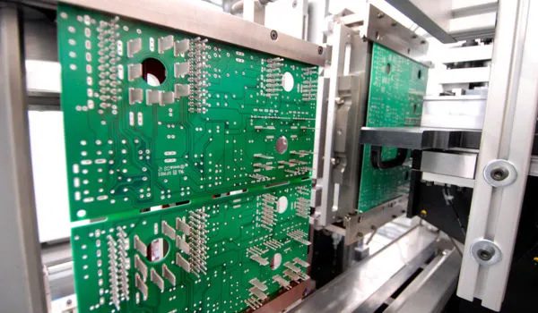
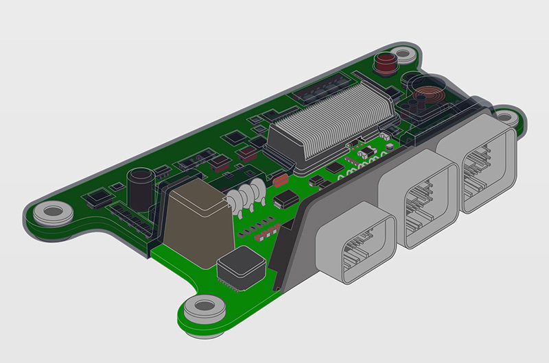
PCB overmolding is a mature and widely used electronic packaging manufacturing process. It is primarily used to enhance the reliability and lifespan of PCBA in complex and harsh environments. This technology utilizes injection molding to encapsulate the entire functional PCB within a high-strength polymer shell. Without affecting electrical performance, it significantly enhances mechanical strength, moisture resistance, chemical corrosion resistance, and environmental protection.
As electronic products continue to evolve towards miniaturization, high integration, and high reliability, PCB overmolding has become an indispensable key process in industrial electronics, automotive electronics, medical equipment, and outdoor applications. By forming a robust and precisely fitted protective structure around the PCB, this technology not only provides electrical insulation and structural support but also effectively resists external influences such as vibration, shock, dust, and moisture.
The following will systematically analyze the process principles, core advantages, commonly used material selections, and key points that need to be focused on during the engineering design process of PCB overmolding technology. This will help engineers and product designers gain a more comprehensive understanding of the value and application prospects of this packaging technology in modern electronic manufacturing.
What is PCB overmolding?
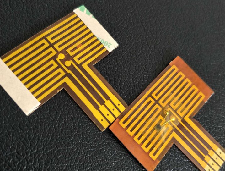
PCB overmolding is a mature and highly reliable manufacturing process. Through this process, a fully assembled PCBA is partially or completely encapsulated in plastic or polymer material. This significantly enhances its mechanical strength, electrical insulation performance, and environmental resistance. This technology is typically implemented using injection molding and is an important solution for the protection and structural integration of electronic products.
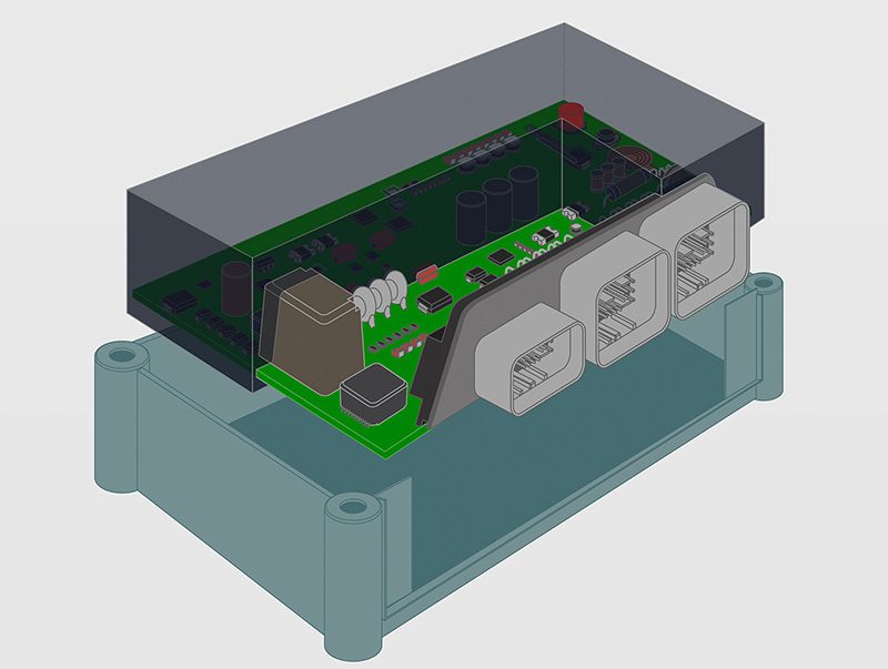
In the actual production process, the pre-assembled PCB is precisely placed in a custom-designed mold cavity. After the mold is closed, molten molding material (usually a thermoplastic or thermosetting polymer) is injected into the mold cavity under high pressure, allowing the material to fully fill the space around the PCB and its components. As the material cools and solidifies, a dense, strong, and highly conforming protective shell is formed on the surface of the circuit board.
This encapsulation layer not only effectively isolates the circuit board from external environmental factors such as moisture, dust, and chemical corrosion, but also absorbs shock and vibration to a certain extent, preventing solder joint or component failure caused by mechanical stress. At the same time, with custom mold design, overmolding allows for highly personalized product shape, interface location, and structural strength, enabling a balance between functionality and aesthetic design.
Material selection is a critical aspect of PCB overmolding. Different polymers offer varying advantages in terms of temperature resistance, flexibility, flame retardancy, and appearance, allowing for customization based on specific application scenarios. Therefore, this process is widely used in fields requiring extremely high reliability, such as automotive electronics, medical equipment, aerospace systems, and industrial and consumer electronic products that need to operate in harsh environments for extended periods.
PCB overmolding technology
Based on the molding process parameters and materials used, PCB overmolding can be mainly divided into two types: low-pressure overmolding and high-pressure overmolding. There are significant differences between the two in terms of injection pressure, temperature conditions, material characteristics, and applicable scenarios. These differences directly affect the structural strength, electronic reliability, and overall manufacturing cost of the final product.
- Low Pressure Overmolding
Low-pressure overmolding uses relatively low injection parameters, with injection temperatures typically controlled between 180–220°C and injection pressure around 100 PSI. This process is mainly suitable for low-viscosity polymer materials, which can uniformly fill the mold cavity under relatively low injection forces.
Due to the significantly lower temperature and pressure during the molding process, low-pressure overmolding is more gentle on the precision electronic components on the PCB. It effectively avoids problems suchs as component deformation, solder joint damage, or internal structural failure. Therefore, this process is very suitable for highly integrated and high-precision PCBA applications, such as sensor modules, medical electronics, and power control boards.
In addition, low-pressure overmolding also has certain advantages in terms of mold wear, energy consumption, and production costs, making it an ideal choice that balances reliability and economy.
- High Pressure Overmolding
High-pressure overmolding uses higher injection parameters, with injection pressure typically reaching 25,000 PSI and injection temperature ranging from 185–300°C. This process is suitable for engineering plastics or composite materials with higher viscosity and stronger mechanical properties.
Compared with the low-pressure process, high-pressure overmolding can provide higher structural strength and superior sealing performance. It is suitable for products requiring high impact resistance, wear resistance, and casing rigidity. However, due to the high injection pressure and temperature, this process is not suitable for PCBs containing fragile or miniature electronic components. Excessive mechanical stress may cause component damage or even render the entire PCBA unusable.
At the same time, high-pressure overmolding requires higher mold precision and manufacturing conditions, and the overall production cost is also relatively higher. Therefore, this process is usually used in applications where structural integrity and environmental protection requirements are extremely high, but the electronic components are relatively simple.
Why is overmolding applied to PCB?
Although overmolding adds to manufacturing costs, its advantages in protection, reliability, and added product value make it worthwhile in many applications. By forming a dense polymer shell around the PCBA, this process significantly improves the lifespan and stability of the circuit board in challenging environments.
- 1. Significantly Enhanced Environmental Protection
Overmolding completely seals the PCB within a protective layer. This effectively blocks dust, moisture, chemical corrosives, and liquid ingress, reducing the risk of failure due to environmental factors. Depending on the chosen materials and structural design, overmolding solutions can achieve protection levels up to IP69, making them particularly suitable for outdoor, industrial, and automotive applications.
- 2. Improved Mechanical Strength and Vibration Resistance
The overmolding material enhances the overall tensile strength of the structure and provides stress relief for solder joints and critical areas (such as around connectors), reducing the risk of damage from impact and vibration. Flexible polymers are especially important in automotive and industrial equipment, effectively extending the reliable operating life of the PCB.
- 3. Improved Appearance and Product Consistency
Exposed electronic components often detract from the overall aesthetics of a product and are more susceptible to damage. Overmolding not only hides components and improves the visual appeal but also allows for personalized design in terms of color, texture, and shape, making the product more competitive in the market, especially for consumer electronics and handheld devices.
- 4. Provides Reliable Electrical Insulation
Overmolding materials typically have good insulation properties, preventing electrical risks such as arcing and short circuits, while also improving safety during equipment use and maintenance.
- 5. Supports Highly Customized Designs
Through custom molds, overmolding can integrate grips, anti-slip structures, or functional shapes onto the exterior of the PCB, optimizing ergonomics and product experience without altering the core circuitry.
Common materials used for PCB overmolding
In the PCB overmolding process, material selection is a critical factor in determining the reliability and performance of the final product. The ideal overmolding material must not only provide sufficient mechanical strength but also possess excellent environmental protection and electrical insulation properties to ensure the encapsulated PCB operates stably for extended periods under complex operating conditions.
The following are common and mature material types used in PCB overmolding:
- TPU and TPE
These materials combine flexibility and wear resistance, offering good adhesion to PCB substrates and components. They effectively absorb vibration and impact and are commonly used in wearable devices, handheld terminals, and applications requiring a certain degree of elasticity.
- PA
PA materials offer high strength, high toughness, and excellent chemical and wear resistance, making them suitable for industrial and automotive electronics applications requiring high mechanical performance.
- PC
PC materials are known for their excellent impact resistance and high transparency, making them ideal for LED windows, indicator light areas, or overmolding structures requiring optical transparency.
- PPS
As a high-performance engineering plastic, PPS possesses excellent high-temperature resistance and natural flame retardancy. It maintains stability in high-temperature and corrosive environments and is widely used in automotive electronics and industrial control fields.
- LSR
LSR is suitable for high-temperature and high-reliability applications, offering excellent flexibility, chemical resistance, and sealing performance. It is commonly used in medical devices, sensors, and electronic product packaging in harsh environments.
Key advantages of PCB overmolding
Overmolding, the integral encapsulation of a PCB, significantly improves reliability, structural strength, and product design, making it a widely adopted packaging solution for high-reliability electronic products.
- Environmental Protection
Overmolding achieves high-level IP protection, effectively isolating moisture, dust, chemicals, and other contaminants, significantly reducing the risks of corrosion, water leakage, and short circuits, ensuring long-term stable operation of the circuit board in harsh environments.
- Mechanical Strength
Through an integrated injection-molded structure, the PCB and housing are tightly bonded, forming a robust whole that effectively resists impact, vibration, drops, and mechanical stress. External loads are evenly distributed, helping to extend product lifespan.
- Electrical Insulation and Protection
Overmolding materials typically possess excellent dielectric properties, effectively preventing arcing, leakage, and short-circuit risks; in specific designs, combined with functional materials, EMI/RFI electromagnetic shielding can be achieved, improving system electromagnetic compatibility.
- Simplified Assembly Process
Overmolding integrates the housing, sealing structure, mounting points, and even connectors into a single component, reducing the number of parts and assembly steps, thereby improving production consistency and reducing overall manufacturing costs.
- Enhanced Design Results
Injection molding supports complex structures and ergonomic designs, allowing for the simultaneous implementation of functional and aesthetic elements such as buttons, labels, and handles during the encapsulation stage. This provides consumer electronics, industrial equipment, and automotive electronics with more distinctive and value-added design possibilities.
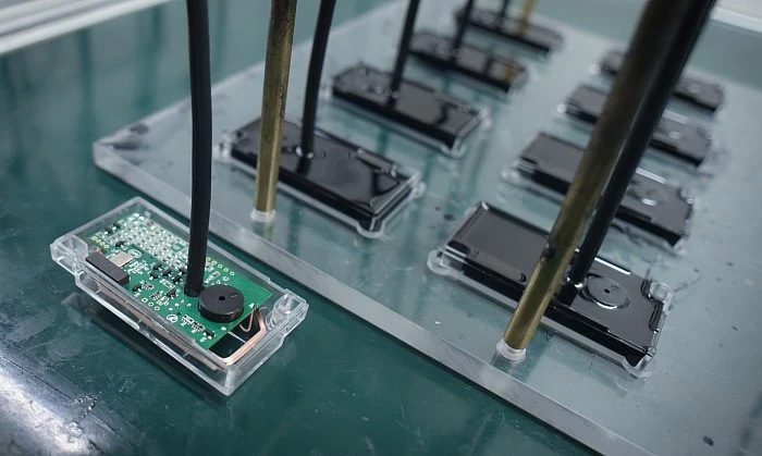
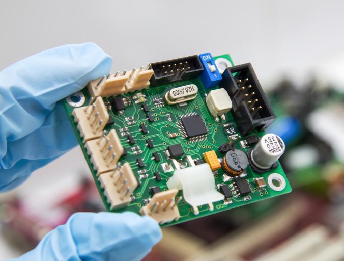
How to protect precision components in PCB overmolding
During PCB overmolding, the high temperatures and pressures of injection molding can pose potential risks to precision electronic components such as chips, sensors, and connectors. Therefore, injection molding manufacturers with experience in electronic packaging typically employ various engineering methods to ensure the safety and reliability of PCBs.
- Low-Pressure Overmolding Technology
By using specialized thermoplastic materials with low melting points and low injection pressures, the mechanical stress and thermal shock to the PCB during molding can be significantly reduced. This method is particularly suitable for circuit boards containing precision components or tiny solder joints.
- Pre-Encapsulation Protection
Before formal overmolding, sensors, MEMS devices, or highly sensitive components can be pre-protected using soft gels or local encapsulation materials to prevent them from being directly subjected to high-pressure impacts during injection molding.
- Mold Structure Design
By introducing high-precision venting channels into the mold, smooth flow of molten material and rapid air expulsion are ensured. Simultaneously, silicone or rubber cushioning structures are placed in critical contact areas to effectively prevent components from being subjected to concentrated pressure.
- Process Parameter Control
Experienced molding engineers will strictly control the melt temperature, injection speed, and pressure profile to ensure that the material is uniformly and smoothly coated around the PCB, avoiding localized stress concentration or thermal damage.
Best Practices for PCB Overmolding Design
In PCB overmolding projects, the rationality of the initial design directly determines the molding quality, reliability, and overall cost. The following design principles can effectively reduce manufacturing risks and improve product consistency and yield.
- Optimize Wall Thickness Design
Minimizing the overall height of components on the PCB helps reduce the thickness of the overmolding layer, allowing the material to cool faster and more evenly in the mold cavity, thereby reducing the risk of internal stress and deformation.
- Critical Functional Component Layout
Connectors, indicator lights, buttons, and other interactive or interface components should be preferentially placed in the PCB edge area to ensure direct exposure or easy secondary assembly and use after overmolding, avoiding complex post-processing.
- Introduce Mold Interlocking Structures
Through interlocking features such as undercuts, through holes, and anchoring grooves, the mechanical bonding force between the PCB and the overmolding material is strengthened, preventing peeling under vibration or thermal cycling conditions.
- Control Component Spacing
Properly setting component spacing can effectively limit material impact and PCB bending during injection molding, improving overall structural stability, especially suitable for high-density PCBA.
- Clearly define the Dam design area
Clearly marking the locations where molten plastic needs to be blocked during the design phase can prevent molten plastic from entering sensitive areas such as connector contacts, sensor windows, or test points.
Applications of PCB overmolding
PCB overmolding technology is widely used in electronic products where reliability, environmental adaptability, and structural strength are extremely important, ensuring stable operation of equipment under complex conditions.
- Automotive Electronics
Used in various sensors, control units, and connectors, it effectively resists vibration, moisture, and temperature variations, meeting automotive-grade reliability requirements.
- Consumer Electronics
Widely used in smartphones, wearable devices, and other products, enhancing the overall waterproofness, durability, and compactness.
- Medical Equipment
Suitable for diagnostic equipment, portable monitors, and other applications, ensuring stable operation of electronic systems and providing good resistance to body fluids and cleaning.
- Industrial Equipment
Provides dustproof, moisture-proof, and mechanical stress-resistant protection in automated equipment, industrial sensors, and control systems, adapting to harsh industrial environments.
- Aerospace and Defense
Used in avionics and military communication equipment, meeting the requirements for high reliability and long-term stable operation in extreme environments.
- Network Equipment
Used in routers, switches, and outdoor communication equipment, enhancing environmental protection capabilities and ensuring signal stability.
- Home Appliances and Smart Home
Provides structural protection in washing machines, refrigerators, and smart control modules, extending product lifespan.
Choose a suitable PCB supplier
PCB overmolding demands extremely high levels of process control and manufacturing experience. As a professional PCB manufacturing and packaging service provider, Thindry possesses mature overmolding technology and a comprehensive process system. We assist customers in selecting appropriate materials and molding solutions based on product application environments and performance requirements.
Thindry effectively reduces the impact on the PCB and components during the molding process through precision mold design, strict temperature and pressure control, and a complete testing process. This ensures that products meet high standards in reliability, environmental protection, and consistency. Thindry provides one-stop technical support, enabling customers to significantly shorten development cycles, reduce manufacturing risks, and accelerate the smooth transition to mass production.


0 Comments