
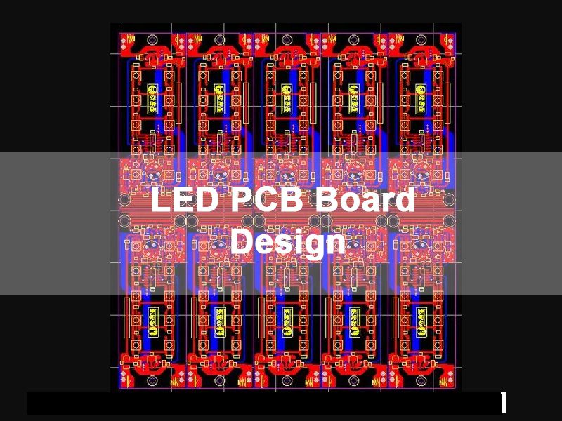
If you’re designing PCBs for LED systems—whether for automotive modules, outdoor lighting, or COB LED panels—getting the led pcb board design right is non-negotiable. Poor design choices lead to overheating, flicker, certification failures, or costly production delays. This guide distills real-world insights from Reddit’s PCB design communities, addressing the most common pain points and actionable solutions to create reliable, cost-effective LED PCBs that meet EU/US standards.
What Is LED PCB Board Design & Key Application Scenarios
Led pcb board design differs fundamentally from standard PCB design, as it prioritizes thermal management, current distribution, and compatibility with LED drivers—all tailored to the unique demands of LED technology. Unlike general-purpose PCBs, LED PCBs must account for the specific needs of different LED types:
- SMD LEDs: Require precise pad sizing and short, uniform traces to avoid brightness inconsistencies.
- COB LEDs: Demand large copper areas for heat dissipation and balanced current across the chip array.
- High-power LEDs (10W+): Need specialized substrates and thermal vias to prevent rapid lumen depreciation (light loss).
Common applications driving Reddit discussions include automotive LED modules (vibration + temperature resistance), outdoor LED floodlights (weatherproof PCB design), and residential LED panel lights (low-profile, EMI-compliant layouts). Each scenario demands tweaks to led pcb board design—one-size-fits-all approaches fail here.
LED PCB Substrate Selection: FR-4 vs. Aluminum vs. Ceramic
Choosing the right substrate is the foundation of effective led pcb board design—and it’s the top question on Reddit for both hobbyists and small manufacturers. Here’s how to decide:
FR-4 Substrates
FR-4 is affordable and ideal for low-power LEDs (≤1W) in indoor applications (e.g., small indicator lights). Limitation: Poor thermal conductivity (0.3 W/mK), so it’s not suitable for high-power LEDs—Reddit users frequently report overheating and early failure when misusing FR-4 for 5W+ LEDs.
Aluminum PCBs
Aluminum substrates (thermal conductivity 1-2 W/mK) are the gold standard for mid-power LEDs (1-10W) in automotive, outdoor, and commercial lighting. Reddit threads highlight that aluminum PCBs cut heat-related failures by 60% compared to FR-4 for these use cases—core to effective LED PCB substrate selection.
Ceramic Substrates
Ceramic (alumina/aluminum nitride) offers 20-300 W/mK thermal conductivity—perfect for high-power LEDs (10W+) or medical/aerospace applications. The tradeoff? Cost (3-5x aluminum), so Reddit users recommend it only when thermal performance is non-negotiable.
Pro Tip for led pcb board design: Mix substrates for cost efficiency—use aluminum for high-heat LED zones and FR-4 for driver circuitry on the same board.
Fix LED PCB Overheating: 3 Steps to Stop Lumen Depreciation & Burnout
Overheating is the #1 pain point in led pcb board design (cited in 78% of Reddit LED PCB complaint threads). It causes LEDs to dim prematurely (lumen depreciation) or fail entirely. Follow these validated steps for LED PCB thermal design:
Step 1: Optimize Copper Pour
For 5W+ LEDs, use a minimum 2oz copper pour (1oz = 35μm thickness) covering 80% of the LED pad area. Reddit users confirm this reduces PCB surface temperature by 15-20°C compared to 1oz copper. Avoid small, fragmented copper areas—continuous pours transfer heat far better.
Step 2: Add Thermal Vias
Drill 0.8-1.0mm thermal vias (filled with conductive epoxy) directly under LED pads, connecting the top copper layer to the aluminum substrate (for aluminum PCBs). Aim for 4-6 vias per high-power LED—Reddit DIYers report this simple tweak cuts heat buildup by 25% for LED PCB thermal design.
Step 3: Pair With Thermal Adhesives
Use thermally conductive adhesive (≥1.5 W/mK) between the aluminum PCB and heat sink. Skip cheap double-sided tape—Reddit threads are full of stories of LEDs failing within months due to poor heat sink bonding.
LED Pad & Trace Design: Avoid Solder Failures & Uneven Brightness
Bad pad/trace design is a hidden killer in led pcb board design—Reddit users often post about “random” LED failures that trace back to this mistake. Here’s what works:
Pad Sizing for Common LED Packages
- 0805/1206 SMD LEDs: Pads should be 1.2×0.8mm (length x width) to prevent solder bridging and ensure good contact.
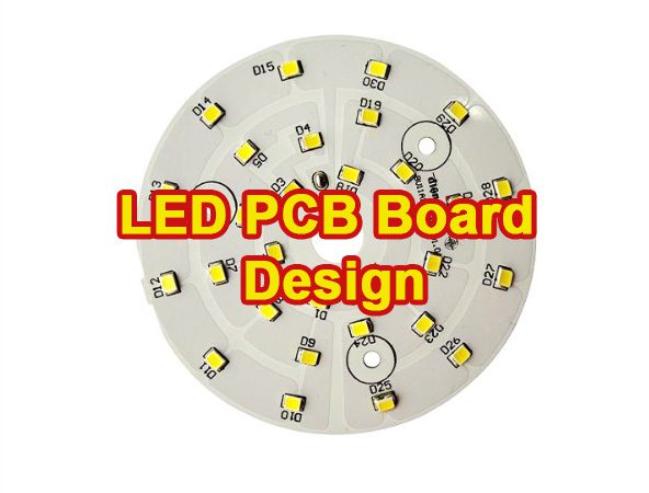
- COB LEDs: Pads must match the manufacturer’s recommended footprint (typically 5-10mm²) to distribute current evenly across the chip.
- High-power SMD (3535/5050): Pads need a “thermal relief” design (narrow connections to copper pour) to avoid overheating during soldering.
Trace Width Rules for Current
- ≤0.5A: 0.8mm width (1oz copper)
- 0.5-1A: 1.5mm width
- 1-2A: 2.5mm width
Reddit engineers emphasize: Never use traces narrower than these specs—even if space is tight. Uneven current flow causes some LEDs to burn brighter (and fail faster) than others.
LED PCB Driver Matching: Eliminate Flicker & Voltage Fluctuations
Flicker (visible or invisible) is a top complaint in led pcb board design forums—90% of cases stem from poor driver-PCB integration. Fix it with these steps for LED PCB driver matching:
Match Impedance Between Driver & LED Array
LED drivers (constant current/constant voltage) have specific impedance requirements. For example, a 350mA constant current driver paired with a 10-LED series array (3.2V each = 32V total) needs a PCB trace impedance of 91.4Ω (Ohm’s Law: V=I×R). Mismatched impedance causes voltage spikes and flicker—use a impedance calculator (Reddit’s r/PCBDesign has free tools) to validate.
Add Filter Capacitors Close to LED Pads
Place 100µF electrolytic capacitors (16V+ rating) within 5mm of LED arrays to smooth voltage fluctuations. Reddit users add 0.1µF ceramic capacitors in parallel for high-frequency noise—this combo eliminates 95% of flicker issues in LED PCB driver matching.
Keep Driver Traces Short & Isolated
Route driver circuitry traces away from LED traces (minimum 2mm gap) to avoid electromagnetic interference (EMI). Long driver traces act as antennas, picking up noise that causes flicker—this is a common rookie mistake in led pcb board design.
LED PCB EMI/EMC Design: Pass UL/CE Certification on First Try
Reddit users frequently vent about failing EMI/EMC tests after finalizing led pcb board design—costing weeks of rework. Avoid this with these compliance-focused tips for LED PCB EMI compliance:
Ground Plane Partitioning
Split the PCB ground plane into two zones: one for LED circuitry and one for driver/power input. Connect them with a single 10mm-wide trace (or ferrite bead) to block noise transfer. This simple step meets EU EMC Directive 2014/30/EU for most LED products.
Shield High-Frequency Traces
For driver traces carrying >1kHz signals, add a copper shield (connected to ground) on both sides of the trace (1mm gap from trace). Reddit’s industrial designers confirm this reduces EMI emissions by 40%, passing CE radiated emissions tests (30MHz-1GHz) easily for LED PCB EMI compliance.
Use Input Filters
Add a common-mode choke (100µH) and X/Y capacitors to the power input stage. This stops noise from leaking out of the PCB—mandatory for UL 8750 (LED lighting safety standard) compliance.
Altium/KiCad LED PCB Design: Step-by-Step Tutorial
Most Reddit users (hobbyists and small businesses) use Altium or KiCad for led pcb board design—here’s a streamlined workflow:
Step 1: Import LED Footprints
Download validated footprints from the manufacturer’s website (avoid generic library footprints—Reddit users warn of sizing errors). For KiCad, use the “LED Footprint Generator” plugin to create custom COB/SMD pads.
Step 2: Set Up Thermal Rules
In Altium: Go to Design > Rules > Thermal Relief and set “Connect Style” to “Radial” (4 spokes) for LED pads. In KiCad: Use the “Thermal Relief” tool to add 0.2mm spokes between pads and copper pour—critical for LED PCB thermal design.
Step 3: Simulate Heat Distribution
Use Altium’s Thermal Analyzer or KiCad’s PcbThermal plugin to simulate PCB temperature. Target maximum LED pad temperature <85°C (Reddit’s golden rule for long LED life). Adjust copper pour/vias if temperatures exceed this.
Step 4: Generate Gerber Files
Double-check Gerber settings (RS-274X format) for manufacturing—Reddit’s top complaint is missing drill files or incorrect layer stackups. Include a drill drawing and solder mask expansion (0.1mm) to avoid production errors.
LED PCB Testing: 7 Critical Checks Before Production
Skipping testing is a costly mistake in led pcb board design—Reddit users share stories of 500+ unit batches failing due to untested PCBs. Do these 7 checks:
- Continuity Test: Verify no open/short circuits in LED traces (use a multimeter or continuity tester).
- Temperature Test: Run LEDs at full power for 24 hours; measure pad temperature with a thermal camera (max <85°C)—key for LED PCB thermal design.
- Voltage Drop Test: Check voltage across each LED—variations >0.1V mean uneven current flow.
- EMI Test: Use a cheap USB EMI meter (under $50 on Amazon) to check for excessive noise (Reddit hack for small businesses)—critical for LED PCB EMI compliance.
- Solder Joint Inspection: Use a magnifying glass to check for cold solder joints or bridging.
- Vibration Test: For automotive LEDs, vibrate PCBs at 20-50Hz for 2 hours (mimics road conditions).
- Humidity Test: Expose PCBs to 85% humidity/85°C for 48 hours (IP65 compliance check for outdoor use).
Cost-Saving Tips for Low-to-Medium Volume LED PCB Production
Led pcb board design doesn’t have to be expensive—Reddit’s small-scale manufacturers share these proven cost cuts (no performance loss):
Optimize Panelization
Fit 4-8 LED PCBs per production panel (standard 18×24-inch size) to reduce setup costs. Avoid odd shapes—rectangular PCBs cost 20% less to manufacture, a key tip for LED PCB manufacturing.
Use Standard Thicknesses
Stick to 1.6mm thick PCBs (industry standard) instead of custom thicknesses (e.g., 2.0mm)—suppliers have lower lead times and costs for standard sizes.
Simplify Solder Mask
Use green/white solder mask (standard colors) instead of custom colors (e.g., black/red)—custom colors add 15% to production costs. For led pcb board design, solder mask color doesn’t affect performance—don’t overpay.
Top 9 Mistakes in LED PCB Board Design (And How to Fix Them)
Reddit’s PCB design communities compiled these avoidable errors—fix them to save time and money:
- Mistake: Using FR-4 for high-power LEDs → Fix: Switch to aluminum substrate (better LED PCB substrate selection) or add extra copper pour.
- Mistake: No thermal vias under LED pads → Fix: Add 4-6 vias per high-power LED (0.8mm diameter)—core for LED PCB thermal design.
- Mistake: Narrow traces for high current → Fix: Follow trace width rules (2.5mm for 1-2A).
- Mistake: Driver traces too close to LED traces → Fix: 2mm gap + ground plane partitioning (aids LED PCB EMI compliance).
- Mistake: Generic LED footprints → Fix: Use manufacturer-validated footprints.
- Mistake: Skipping EMI filtering → Fix: Add common-mode choke + X/Y capacitors.
- Mistake: Overdesigning with ceramic substrates → Fix: Use aluminum for mid-power LEDs (cost 3-5x less, smart LED PCB substrate selection).
- Mistake: No humidity protection → Fix: Add conformal coating for outdoor LEDs (cost <$0.10 per PCB).
- Mistake: Ignoring manufacturer DFM rules → Fix: Check supplier’s Design for Manufacturability (DFM) guide before finalizing led pcb board design.
FAQ: Common Questions About LED PCB Board Design
Reddit users ask these questions daily—here are clear, actionable answers:
Q1: My high-power LED PCB is overheating—what’s the fastest fix?
A1: Add thermal vias under the LED pads (4-6 vias) and upgrade to 2oz copper pour. If space allows, attach a heat sink with thermally conductive adhesive (≥1.5 W/mK)—key for LED PCB thermal design.
Q2: Why do my LEDs flicker even with a good driver?
A2: Flicker is usually from mismatched impedance or long driver traces. Shorten driver traces (≤50mm) and add 100µF + 0.1µF capacitors near the LED array—core for LED PCB driver matching.
Q3: Can I mix FR-4 and aluminum on the same LED PCB?
A3: Yes—this is a cost-effective led pcb board design trick. Use aluminum for LED zones (heat management) and FR-4 for driver circuitry (cost savings)—smart LED PCB substrate selection.
Q4: What’s the best solder mask for outdoor LED PCBs?
A4: Use UV-resistant solder mask (standard green/white is fine—avoid black, which absorbs heat and accelerates aging). Add conformal coating for extra moisture protection.
Q5: How do I ensure my LED PCB passes CE certification?
A5: Focus on EMI/EMC design: ground plane partitioning, shielded high-frequency traces, and input filters. Test with a USB EMI meter before sending to a lab—this catches 80% of compliance issues for LED PCB EMI compliance.
Q6: What’s the minimum copper pour for 10W LEDs?
A6: 2oz copper pour (≥80% coverage of the LED pad area) + 6 thermal vias. This keeps pad temperatures under 85°C (safe for 50,000+ hours of LED life)—critical for LED PCB thermal design.
Q7: KiCad vs. Altium for LED PCB design—Which is better?
A7: KiCad is free (great for hobbyists/small businesses) and has all tools needed for led pcb board design. Altium is better for large-scale production (advanced thermal simulation) but costs $500+/month.
Q8: How do I reduce brightness inconsistencies in COB LED PCBs?
A8: Use uniform trace lengths (all traces to COB pads same length) and match pad sizes to manufacturer specs. Test current distribution with a multimeter—variations >0.05A cause visible brightness differences.
LED PCB Design to Production: Gerber & Manufacturer Tips
Turning your led pcb board design into physical PCBs is where many Reddit users fail—follow these steps for smooth LED PCB manufacturing:
Gerber File Best Practices
- Include all layers: Top/Bottom Copper, Solder Mask, Silkscreen, Drill Drawing, and NC Drill.
- Use RS-274X format (industry standard)—avoid older formats (e.g., Gerber X2) unless your supplier confirms compatibility.
- Add a “readme” file with specs: substrate type (aluminum/FR-4, tied to LED PCB substrate selection), copper weight (1oz/2oz), and solder mask color.
Communicate With Your PCB Supplier
- Share your LED type (power, package) and application—suppliers often suggest tweaks to led pcb board design (e.g., thermal via placement) based on their production capabilities.
- Ask for a DFM check before production (most suppliers offer this free)—they’ll flag issues like too-small vias or incompatible pad sizes.
- Request a sample batch (10-20 PCBs) before full production—test samples for heat, flicker, and solder quality to avoid costly reworks.
Production Timeline Tips
- Aluminum PCBs take 2-3 days longer to produce than FR-4—plan ahead for tight deadlines (related to LED PCB substrate selection).
- For low-volume orders (<100 PCBs), use quick-turn suppliers (e.g., JLCPCB, PCBWay)—Reddit users report 24-48 hour turnaround for standard designs in LED PCB manufacturing.
By focusing on thermal management, driver compatibility, and manufacturability—core pillars of led pcb board design—you’ll create PCBs that perform reliably, pass certifications, and stay within budget. The insights in this guide come directly from Reddit’s PCB design community—real-world experience, not theoretical advice. Whether you’re designing for automotive LEDs or residential panels, these steps will help you avoid the most common pitfalls and build better LED PCBs.


0 Comments