
Introduction: The Ubiquitous Smart Screen and Its Foundational Technology
From the smartphones in our pockets to the smart TVs in our living rooms, from automotive smart central consoles to industrial control equipment in factories, smart screens have become an indispensable user interface for modern electronic devices. However, behind these colorful and responsive displays lies a critical component—the PCB (Printed Circuit Board). Serving as the support structure for electronic components and the provider of electrical connections, the PCB acts as the “skeleton” and “neural network” of a smart screen, directly determining the quality of the display effect and the reliability of the device. In an era of continuous miniaturization and high integration of smart devices, even a seemingly simple smart screen conceals complex PCB design and manufacturing technologies. This article will provide an in-depth analysis of the structural characteristics, design challenges, manufacturing processes, and future trends of smart screen PCBs, revealing how this green board becomes the core engine for display interaction in modern electronics.
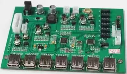
Basic Structure of PCBs and Special Requirements for Smart Screens
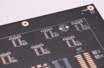
The basic structure of a PCB includes the substrate material, conductive layers (copper foil), solder mask, and silkscreen layer. The substrate typically uses glass fiber reinforced resin (e.g., FR-4) as the insulating material, with precise copper traces formed on the surface through etching to connect various electronic components. The solder mask (usually green solder resist ink) covers the traces for insulation and protection, while the silkscreen layer is used for marking component locations and identification information.
Smart screen PCBs have higher specific requirements compared to standard PCBs. They must simultaneously fulfill three core demands: “stable display driving,” “sensitive touch signaling,” and “multi-module coordination.” Structurally, smart screen PCBs often adopt 4-8 layer or even higher layer count multilayer board designs to achieve higher wiring density and better signal integrity. For example, PCBs for smart home central control screens are typically 6-8 layer boards, isolating pixel data lines, control signal lines, and power lines on different layers to avoid crosstalk.
Smart screen PCBs also require high flatness (warpage less than 0.3%) and high stability to ensure the soldering quality and long-term reliability of surface-mounted components. Furthermore, to adapt to different application scenarios, smart screen PCBs have evolved into various forms, including rigid PCBs, flexible PCBs (FPC), and rigid-flex boards, suitable for standard devices, foldable devices, and high-end medical/aerospace equipment, respectively.
Core Functional Modules of Smart Screen PCBs
A smart screen PCB is a highly integrated system comprising several core modules with distinct functions, each having unique design requirements.
The display driver module is the core of the smart screen PCB, responsible for processing video signals from the main control chip and driving the display panel. The heart of this module is the TCON (Timing Controller) chip, which converts LVDS or eDP video streams from the mainboard into driving signals understandable by the LCD panel, such as Horizontal Sync (HSYNC), Vertical Sync (VSYNC), Data Enable (DE), and Clock (CLK). Modern TCON chips are highly integrated; besides basic timing control functions, they often incorporate EDID storage interfaces, I²C/SPI configuration channels, backlight control outputs, and even support technologies like Variable Refresh Rate (VRR).
The touch control module is key to human-machine interaction. Smart screens typically use capacitive touch technology, detecting minute capacitance changes (usually 0.1-1pF) through “touch sensing electrodes” and “signal processing traces” on the PCB. To ensure touch sensitivity, electrode spacing must be highly uniform (0.5mm ± 0.02mm), and the distance from display driver traces should be ≥ 2mm to prevent display signal interference. Signal transmission traces often employ a “shielded twisted pair” design to reduce external electromagnetic interference.
The power management module provides stable and reliable multiple voltage rails for various components of the smart screen. A typical TFT-LCD panel requires VDD/VCC logic supply (1.8V or 3.3V), VGH gate turn-on voltage (+15V to +20V), VGL gate turn-off voltage (around -10V), and analog supply AVDD, among others. The power-up sequencing of these voltages is critical, as incorrect timing can cause latch-up effects, leading to permanent damage.
The interface and protection circuit module handles connections to external devices and provides electrostatic discharge (ESD) protection. Interface protection circuits typically use high-voltage capacitors (withstand voltage of at least 1.5KV) placed at I/O connectors or key signal locations to prevent ESD damage.
Key Design Challenges and Solutions for Smart Screen PCBs
Smart screen PCB design faces multiple technical challenges, requiring engineers to comprehensively consider factors such as signal integrity, power integrity, thermal management, and electromagnetic compatibility.
High stability of display driver lines is a primary challenge. Taking a 10.1-inch LCD screen as an example, it can have over 200 pixel data lines, each requiring signal delay controlled within ±1ns; otherwise, “screen ghosting” may occur. The solution involves adopting “serpentine routing” technology to precisely control the length of each data line (length mismatch ≤ 0.5mm), ensuring all pixel signals arrive at the display panel synchronously. Simultaneously, the power supply lines for the display driver chip require separate design, with “100μF + 0.1μF” filter capacitor combinations soldered to suppress power supply noise.
High sensitivity of touch signals demands precise design. For accurate touch detection, touch sensing electrodes need uniform layout and should use “low-resistance copper foil” (resistivity ≤ 1.72×10^-8 Ω·m) to reduce signal transmission loss. Touch signal traces should be routed away from high-frequency noise sources, with shielding layers added if necessary. Case studies show that adjusting the spacing between touch traces and display traces from 1mm to 2.5mm and using shielded twisted pairs can reduce touch false trigger rates from 10% to 0.3%.
Multi-module co-existence compatibility is a difficulty in complex system design. Smart screens typically integrate multiple modules like display, touch, WiFi/Bluetooth, voice, and camera, each with different electrical characteristics (high-frequency signals, analog signals, digital signals). An effective solution is “partitioned design + ground isolation”: dividing functional areas on the PCB, separated by “ground copper foil isolation belts” (width ≥ 3mm); the grounding system employs a “star grounding” method, where all module ground lines converge to a single ground point. This design avoids module conflicts. For instance, after implementing this scheme, the voice recognition accuracy of a certain high-end central control screen improved from 85% to 98%.
High-speed signal integrity is key to ensuring image quality. High-speed differential signals like LVDS/eDP require strict control of differential impedance at 100Ω ± 10%, achieved through fine impedance control techniques. Designs should use a four-layer board structure, route high-speed signals on the outer layers referencing a solid ground plane, and avoid crossing split planes. The length mismatch within differential pairs should be less than 5mm, and arcs or 45-degree miters should be used for length matching to avoid impedance discontinuities caused by 90-degree angles.
PCB Manufacturing Processes and Special Treatments for Smart Screens
PCB manufacturing is a complex precision process involving multiple key steps. Due to their specific requirements, smart screen PCBs need more specialized treatments and process controls.
Substrate preparation and inner layer imaging form the initial stage. After cutting the copper-clad laminate (e.g., FR-4) to the required size, the circuit pattern is transferred onto the copper foil through photolithography (exposure, development), followed by etching away excess copper with chemical solutions (e.g., ferric chloride) to form conductive traces. For High-Density Interconnect (HDI) boards used in smart screens, this process demands higher precision and control over line width/spacing.
Lamination and drilling are critical for multilayer board manufacturing. Inner layer cores and prepreg sheets are stacked and laminated into a multilayer structure under high temperature and pressure. Through-holes, blind vias, and buried vias are then created via mechanical or laser drilling to achieve interlayer connections. Smart screen PCBs often utilize laser-drilled microvias (aperture < 0.1mm) to meet high-density wiring requirements.
Hole metallization and plating make the vias conductive. Chemical copper deposition and electroplating metallize the via walls, forming electrical connections between layers. The quality of this process directly relates to signal transmission reliability, which is particularly important for high-speed display signals.
Surface finish is a key step ensuring soldering quality and reliability. Smart screen PCBs often employ the ENIG (Electroless Nickel Immersion Gold) process due to its strong oxidation resistance and high flatness, making it suitable for high-density pads. Other optional processes include HASL (Hot Air Solder Leveling) and OSP (Organic Solderability Preservative).
Solder mask and silkscreen application provide the final protection and identification. The solder mask (green lacquer) covers the traces to prevent short circuits, while the silkscreen layer prints component identifiers, polarity marks, etc. For smart screen PCBs, the precision of solder mask openings is crucial for the soldering quality of fine-pitch components like FPC connectors.
Special process treatments include via tenting, filling, and plugging techniques to improve assembly yield and reliability. For example, tented vias cover the pads at both ends of the hole with solder mask, effectively sealing the openings; plugged vias fill the through-holes with non-conductive epoxy paste to prevent solder wicking during assembly.
Correlation Between Material Selection and Smart Screen Performance
Material selection directly impacts the performance, reliability, and cost of smart screen PCBs. Different application scenarios require different material strategies.
Substrate material is the foundation of the PCB. FR-4 epoxy resin glass fiber boards are the most common material, offering good mechanical strength and electrical properties, suitable for most smart screen applications. For high-frequency and high-speed applications, such as 5G devices, materials with low dielectric loss like PTFE (Polytetrafluoroethylene) are needed to reduce signal transmission loss.
Copper foil is the key material forming conductive traces. PCBs primarily use rolled copper foil and electrolytic copper foil. Rolled copper foil has tighter molecular structure, smoother surface (beneficial for high-speed signal propagation), better flex endurance, and is suitable for flexible PCBs and high-frequency circuits. Copper foil thickness is usually expressed in ounces (oz), where 1oz copper foil is approximately 1.4 mils (35μm) thick.
Substrate performance indicators significantly affect smart screen performance. The Dielectric Constant (Dk) affects signal propagation speed, while the Dissipation Factor (Df) determines signal transmission loss. High-speed smart screen PCBs should select materials with low Dk and Df values. The Glass Transition Temperature (Tg) indicates the temperature at which the resin transitions from a rigid to a soft state; high-Tg laminates (greater than 170°C) are suitable for multilayer boards and high-temperature application scenarios.
Flexible materials like Polyimide (PI) are key for flexible screens and foldable devices, allowing the PCB to bend or even fold. These materials require high flex endurance and stability to meet the demands of repeated bending.
Eco-friendly materials represent a future trend. With growing environmental awareness, halogen-free substrates, lead-free HASL, and other eco-friendly materials and processes are gradually becoming widespread, reducing the environmental impact of PCB manufacturing and use.
Industry Applications and Special Considerations for Smart Screen PCBs
Due to their diverse application scenarios, smart screen PCBs have different design priorities and specific requirements across various industries.
In the consumer electronics field (smartphones, tablets), smart screen PCBs pursue thinness, lightness, and high density. These PCBs typically use HDI technology and flexible circuit designs to maximize functional integration within limited space. For instance, the display driver PCB in smartphones is often integrated with the touch controller chip on the same flexible circuit, directly connected to the mainboard.
In the automotive electronics field, automotive display PCBs emphasize high reliability and wide temperature adaptability. Automotive electronics require a wide operating temperature range (-40°C to 85°C or higher) and resistance to vibration and humid environments. Therefore, automotive screen PCBs must use automotive-grade components and pass stringent reliability tests. Power management design is also more complex, needing to consider transient overvoltages and load dump scenarios in the vehicle electrical system.
Smart screen PCBs for industrial control equipment emphasize anti-interference capability and long-term stability. Industrial environments feature complex electromagnetic interference, necessitating reinforced EMC measures in PCB design, such as adding shields and optimizing grounding. Simultaneously, industrial equipment has long expected lifespans, requiring long-term supply stability for the PCB and its components.
Display PCBs in medical equipment focus on signal integrity and safety. Medical displays are often used for diagnostic reference, demanding extremely high image quality and stability. Gamma correction circuits require more precise design, using metal film resistors with 0.5% to 1% tolerance to ensure accurate grayscale performance. Furthermore, critical sections need isolation design to prevent leakage current risks.
Smart home central control screen PCBs need to balance performance and cost. These PCBs typically adopt 6-8 layer designs, supporting multi-module collaboration like display, touch, voice, and camera. To reduce costs, some solutions integrate the CPU and large-capacity memory directly onto the PCB, enhancing boot speed and system performance.
Future Development Trends and Challenges
Smart screen PCB technology continues to evolve, facing new opportunities and challenges. Future development trends are mainly reflected in the following aspects:
High-Density Interconnect (HDI) technology is a key direction for smart screen PCB development. As display resolution increases and devices miniaturize, the demand for PCB wiring density continuously grows. HDI technology utilizes microvias (<0.1mm), laser drilling, and other techniques to meet the need for higher integration in smartphones and 5G devices. The line width/space of advanced HDI boards has shrunk to 0.15-0.1mm, significantly increasing circuit logic density.
The application of high-frequency and high-speed materials is becoming increasingly important with the growth of 5G and high-speed data transmission demands. High-frequency applications require materials with low dielectric constant and low loss factor, such as PTFE, to enhance signal integrity. Future smart screen PCB materials will focus more on high-frequency characteristics while balancing manufacturability and cost.
Flexible display technology is driving the development of flexible PCBs. The rise of foldable devices and wearables requires PCBs that can bend or even fold. Flexible PCBs use flexible materials like polyimide, necessitating special mechanical and electrical design considerations, such as bend resistance and conductor ductility.
Embedded component technology is a frontier direction for PCB miniaturization. Embedding passive components (resistors, capacitors) or even active devices within the PCB internal layers can further increase integration and reduce surface area usage. This technology imposes higher demands on manufacturing processes and materials but opens possibilities for ultra-thin devices.
Green manufacturing and sustainable development are becoming industry consensus. The PCB manufacturing industry is moving towards more environmentally friendly directions, with lead-free HASL, low-toxicity etching solutions, and other eco-friendly processes gradually becoming widespread. In the future, eco-friendly material selection, energy efficiency improvement, and carbon footprint reduction will become important topics for the PCB industry.
3D printed PCB technology, as an emerging additive manufacturing method, holds potential for rapid prototyping. Although it hasn’t yet replaced traditional subtractive processes, 3D printing technology shows promise in rapid prototyping, customization, and small-batch production, potentially changing traditional PCB manufacturing models.
Thermal management challenges intensify with increasing power density. High-brightness, high-refresh-rate displays generate more heat, requiring smart screen PCBs to adopt more effective thermal management strategies, such as thermal vias, metal core substrates, and integrated heat dissipation design.
Increasing system integration is a long-term trend. With advancements in semiconductor technology, more functions are integrated into single chips, but PCBs still need to accommodate higher levels of system integration, such as more tightly combining display drivers, touch controllers, and processors.
Summary
As the core of display interaction in modern electronic devices, the technological substance of the smart screen PCB is far richer than its appearance as a simple green board suggests. From basic connection functions to complex system integration, from simple single-layer designs to high-density multilayer architectures, smart screen PCB technology has evolved into a comprehensive engineering discipline integrating electrical, mechanical, thermal management, and materials science.
Facing growing display demands and complex, varied application environments, the design and manufacture of smart screen PCBs require comprehensive consideration of multiple factors including signal integrity, power integrity, thermal management, and electromagnetic compatibility. Every meticulous design detail—whether it’s synchronous signals achieved through serpentine routing, module synergy from ground isolation, or high-speed transmission ensured by impedance matching—embodies the boundless ingenuity of engineers working within finite spaces.
With the development of 5G, AI, IoT, and flexible display technologies, smart screen PCBs will continue to evolve towards higher density, higher frequency, flexibility, and environmental sustainability. Future smart screen PCBs will not merely be carriers for connecting components but will develop into highly integrated system-level solutions, delivering richer, smoother, and more reliable visual interactive experiences for electronic devices. In this process, material innovation, process advancement, and design methodology upgrades will collectively propel smart screen PCB technology to new heights.


0 Comments