
Introduction: The Evolution of the Industrial Automation Core and the Key Role of PCBs
The development of industrial automation is a history of continuous evolution towards greater efficiency, precision, and intelligence. From the introduction of the “automation” concept in the latter half of the 20th century to reduce human intervention in production processes, to the digital transformation driven by Industry 4.0 in the 21st century, the industrial manufacturing sector has undergone revolutionary changes. Throughout this evolution, motors have consistently played an indispensable role as actuating components, while motor drives—inverters and servo drives—have become key equipment for achieving precise control.
As the core carrier of the inverter, the design and manufacturing quality of the Printed Circuit Board (PCB) directly determines the inverter’s performance, reliability, and service life. As industrial equipment advances towards intelligence, miniaturization, and high power density, industrial inverter PCB design faces multiple challenges, including Electromagnetic Compatibility (EMC), thermal management, and high-density interconnects. Modern industrial inverter PCBs have evolved into highly integrated systems, requiring comprehensive consideration of circuit layout, signal integrity, power delivery, and numerous other factors to meet the demanding application requirements of industrial environments.
This article systematically analyzes the key design points, technical challenges, and solutions for industrial inverter PCBs, providing in-depth and practical technical reference for engineers in related fields.
Core Functions and Architectural Characteristics of Industrial Inverter PCBs
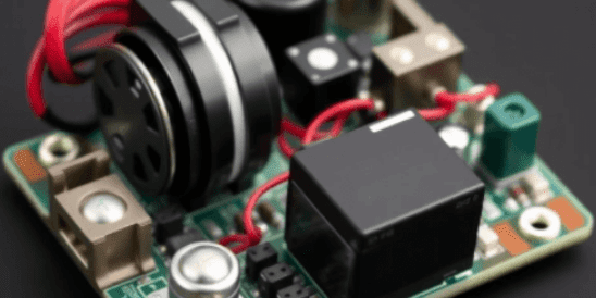
The industrial inverter PCB serves as the nerve center and circulatory system of the inverter, responsible for coordinating the entire equipment’s operation and providing power paths. From a functional architecture perspective, the inverter PCB primarily undertakes three core functions: power conversion, signal processing and control, and communication interfaces.
The fundamental working principle of an inverter involves first converting the mains AC power supply into a DC power supply via a rectifier, and then converting this DC supply into an AC power supply with controllable frequency and voltage via an inverter, thereby achieving precise adjustment of motor speed. This process relies on the coordinated operation of four main sections on the PCB: the rectifier unit, intermediate circuit, inverter unit, and controller.
In terms of technical architecture, modern industrial inverter PCBs are characterized by a high degree of integration. Taking an inverter solution utilizing a Digital Signal Processor (DSP) as an example, its core control unit typically employs specialized chips such as the TMS320LF2406. Through efficient vector control algorithms and PID regulation, it achieves precise motor control. Such digital solutions not only improve control accuracy but also offer good portability and maintainability through source code written in C language.
The architectural characteristics of inverter PCBs are also reflected in their strict layer partitioning: typically divided into the power layer, control layer, and signal layer. The power layer handles high-current paths, requiring sufficient copper thickness and width to withstand high currents. The control layer acts as the “brain” of the inverter, executing complex control algorithms. The signal layer processes various sensor feedback and user commands, requiring high noise immunity. This clearly layered architecture ensures dedicated functionality for each section, minimizing mutual interference.
Key Technical Challenges in Industrial Inverter PCB Design
Industrial inverter PCB design faces multiple technical challenges, with Electromagnetic Compatibility (EMC) being paramount. Industrial high-voltage inverter PCBs (e.g., 11kV class) generate strong Electromagnetic Interference (EMI) under high-frequency switching (above 50kHz). Inadequate EMC design can cause malfunctions in peripheral equipment (e.g., PLCs, sensors). Data indicates that EMC interference exceedances for industrial inverter PCBs surpass 35%, while test pass rates are below 60%, leading to over 5 R&D iteration cycles, significantly increasing development cost and time.
Thermal management is another critical challenge. Power losses during inverter operation cause component temperatures to rise, subsequently affecting performance and service life. The application of high thermal conductivity materials and rational thermal design become crucial for ensuring reliable inverter operation. Especially achieving efficient heat dissipation within compact spaces requires comprehensive consideration of the three heat transfer paths: conduction, convection, and radiation. Often, heat sink fin structures are used to increase surface area, with forced air or liquid cooling employed when necessary.
High-Density Interconnect (HDI) is a challenge increasingly prominent with the trend towards equipment miniaturization. As the intelligence level of industrial equipment increases, more sensor, control signal, and data interfaces need to be incorporated, while internal space becomes more compact. This contradiction demands that PCB designs achieve more functionality within limited space, driving the use of HDI technology and miniature components.
Reliability and environmental adaptability are equally critical challenges that cannot be overlooked in industrial inverter PCB design. Industrial environments often present adverse conditions such as vibration, humidity, dust, and extreme temperature fluctuations. The PCB must operate stably under these conditions. This requires special design considerations across multiple aspects, including material selection, coating protection, and structural reinforcement. For example, using high-Tg FR-4 substrates (Tg ≥ 170°C) ensures the PCB can operate stably long-term above 150°C, and employing copper foil shields reduces radiative interference coupling into signal loops.
PCB Layout and Electromagnetic Compatibility (EMC) Design Optimization
Achieving excellent EMC is one of the core challenges in industrial inverter PCB design. According to the CISPR 22 Class A standard, radiation disturbance limits for industrial equipment are 54 dBμV/m (30-1000MHz), and conducted disturbance limits are 79 dBμV (0.15-0.5MHz). Meeting these stringent standards requires optimization across three dimensions: layout partitioning, filter design, and grounding systems.
Layout Partitioning and Routing Optimization
Rational layout partitioning is the foundation of EMC design. The PCB should be strictly divided into a power section (IGBTs, rectifier bridge), control section (MCU, driver chips), and filter section (common-mode chokes, X/Y capacitors), with spacing between sections ≥ 15mm. A “copper isolation strip” (width ≥ 5mm and grounded) should be placed between the power and control sections to effectively block interference propagation. Key routing measures include: IGBT drive trace lengths should be controlled to ≤ 30mm, width ≥ 2mm (for 2oz copper weight), using parallel routing to reduce loop area (< 100mm²), and avoiding right-angle bends to reduce signal reflections. For signal routing, current sense lines (e.g., Hall sensor outputs) should use twisted pairs (twist pitch ≤ 10mm) and cross power lines perpendicularly where necessary to reduce coupling.
Filter Design and Component Selection
Filter design is a crucial means of suppressing electromagnetic interference. Common-mode choke selection should be based on the power loop current (e.g., 50A), choosing an appropriate model (e.g., 100A common-mode choke) to ensure common-mode interference attenuation ≥ 40dB at high frequencies (e.g., 50kHz). The selection of X capacitors (across Line-Neutral) and Y capacitors (across Line-Ground, Neutral-Ground) is also critical. Typically, an X capacitor of 0.01μF (X2 rating, 275V AC withstand) and Y capacitors of 10nF (Y1 rating, 500V AC withstand) are used, ensuring conducted interference attenuation ≥ 30dB across the 0.15-1000MHz band. Filter placement is equally crucial; the “π-type filter” formed by the common-mode choke and X/Y capacitors should be placed at the power entry point (≤ 20mm from the PCB edge), and the filtered power lines should maintain a spacing ≥ 10mm from the power section.
Grounding Optimization and Impedance Control
The grounding system design directly impacts EMC performance. A combined strategy of “multi-point grounding” (for high frequencies > 10MHz) and “single-point grounding” (for low frequencies < 1MHz) should be adopted. The Power Ground (PGND) and Signal Ground (SGND) should be laid out separately on the bottom layer of the PCB, connecting only at a single point near the power entry (ground connection impedance should be ≤ 0.1Ω). Ground copper pour design is also vital: PGND copper width should be ≥ 10mm (for 4oz copper weight), SGND copper should cover the control section (coverage ≥ 80%), and the number of ground vias should be ≥ 10 per section (via diameter 0.5mm, pitch 2mm) to reduce ground impedance. For particularly sensitive control areas, a “copper shield can” (thickness 0.2mm) can be used; the shield ground impedance should be ≤ 0.5Ω, effectively reducing radiative interference coupling into the signal loop.
Practice proves that good EMC design can reduce inverter PCB radiation disturbance from 65 dBμV/m to 48 dBμV/m (a 26% reduction) and conducted disturbance from 88 dBμV to 72 dBμV (an 18% reduction). The malfunction rate of peripheral PLCs can decrease from 25% to 0.3%, significantly enhancing system reliability.
Connection Technology and Reliability Design for Industrial Inverter PCBs
The connection technology used in industrial inverter PCBs directly affects equipment reliability, maintenance convenience, and overall performance. For industrial application scenarios, PCB connection design must meet four core requirements: reliable electrical connection characteristics, adaptation to space-constrained applications, support for simple and efficient mating operations, and provision of flexible and diverse scalability.
PCB Terminal Block Technology
PCB terminal blocks are key components for achieving reliable connections between cables and the PCB. Taking Phoenix Contact’s PTS and PTSA PCB terminal blocks as examples, they utilize push-in technology, allowing tool-less assembly. The push-in spring connection technology ensures both rapid connection and interconnection reliability. Such terminal blocks also feature horizontal wire entry and integrated test points for quick verification of connection correctness, providing convenience for实际操作. Product series typically offer models from 2 to 24 positions, with pin spacings of 2.5, 3.5, 5, and 7mm, and rated current ranges from 2A to 12A, with rated voltages from 160V to 320V, meeting diverse design requirements.
For measurement and control applications, COMBICON control terminal blocks offer both fixed and pluggable options. Among them, the MKKDS series fixed terminal blocks feature a double-row design for high wiring density, with staggered layers to facilitate wiring operations. This product offers pin spacings of 3.5mm and 5mm, has a compact form factor, and uses screw clamping to ensure secure cable connections, making it well-suited for inverter control circuit interface design.
Data Connection and Board-to-Board Connection Technology
With the increasing reliance on data in industrial automation, reliable data connection interfaces are becoming more widespread in inverters. Board-to-board connectors are an important technical path for achieving high-density PCB interconnections and compact designs. For instance, the FINEPITCH 0.8mm board-to-board connector (FP 0.8 series) utilizes innovative ScaleX technology; its dual-contact design supports a variable mating length of up to 1.5mm, ensuring connection reliability. This connector offers high tolerance compensation, a robust housing structure that effectively protects the contacts, and supports data transmission rates up to 52 Gbps.
Regarding communication interfaces, industrial-grade RJ45 connectors and D-SUB connectors play significant roles in inverters. Industrial-grade RJ45 connectors must meet stringent requirements for industrial environments, offering different configurations such as 90° and 180° mating directions, and single-port and multi-port sockets. D-SUB connectors are suitable for interconnecting signals like inverter encoder interfaces, available in pin and socket types, with 9/15/25/44 positions, and also offering hybrid power+signal interfaces, meeting sealing requirements for industrial applications.
Reliability Design and Environmental Adaptability
The reliability design of industrial inverter PCBs requires comprehensive consideration of environmental adaptability and long-term stability. In material selection, high-Tg FR-4 substrates (Tg ≥ 170°C) should be used to ensure long-term stable operation in high-temperature environments above 150°C. Heavy copper design (e.g., 3OZ, 105μm) can increase current carrying capacity by 3 times while reducing resistance by 60%. Heat dissipation design is also crucial; rational heat sink fin structures can increase the散热面积 by 40%, lowering IGBT junction temperature by over 12°C.
Addressing the specificities of industrial environments, inverter PCBs must also pass a series of rigorous environmental adaptability tests, including temperature cycling (-40°C to +85°C), humidity testing, vibration testing, and dust & water ingress protection tests, ensuring stable operation under various harsh conditions. These reliability design measures collectively ensure the long-term stable operation of industrial inverters in complex industrial environments.
Inverter PCBA Processing Technology and Quality Control
Inverter PCBA (Printed Circuit Board Assembly) processing is the critical step that transforms the design into a physical product, whose quality directly determines the final product’s reliability and performance. The complete PCBA processing workflow includes PCBA design, PCB fabrication, component procurement and inspection, PCBA soldering, finished product inspection and testing, among other stages.
PCBA Processing Workflow
The PCBA design stage involves completing the circuit schematic design, PCB layout and routing, and EMC design. Considering the operational characteristics of inverters, specialized EMC design for the PCB is essential to reduce the impact of electromagnetic interference on the circuit. The PCB fabrication stage involves substrate material selection, drilling, pattern etching, plating, and other processes, ultimately forming the complete circuit board.
Component procurement and inspection are critical; the quality of core components like IGBTs directly affects inverter performance. Currently, European and Japanese companies lead in IGBT R&D and production, such as Infineon Technologies AG (Germany), Mitsubishi Electric Corporation (Japan), and Fuji Electric Co., Ltd. (Japan). Most domestic inverter manufacturers procure these core components through distributors, introducing certain supply chain risks.
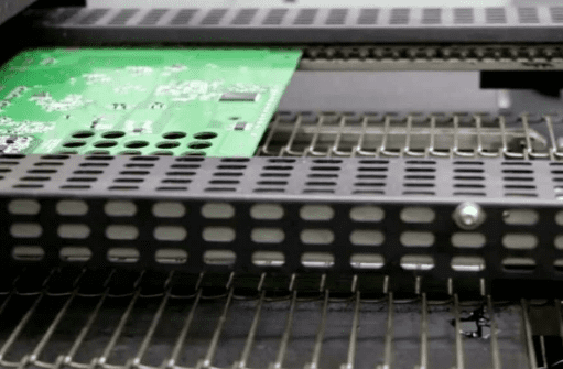
The PCBA soldering stage employs various advanced processes, including Surface Mount Technology (SMT), Ball Grid Array (BGA) packaging technology, wave soldering technology, and laser soldering technology. SMT places electronic components directly onto the PCB surface, enabling miniaturized, high-density, and highly reliable assembly. BGA technology achieves high-density, high-performance packaging through solder ball connections, suitable for high-speed, high-frequency applications.
Quality Inspection and Control
Quality inspection after PCBA processing includes visual inspection, dimensional inspection, electrical performance testing, and reliability testing, among other aspects. Visual inspection ensures the PCBA surface is free from scratches, stains, burns, and other defects. Dimensional inspection ensures the PCBA conforms to design requirements, preventing assembly issues due to dimensional deviations. Electrical performance testing uses specialized instruments to check parameters like voltage, current, resistance, capacitance, and inductance, ensuring performance meets specifications.
Reliability testing evaluates the PCBA’s reliability through various environmental tests such as aging, withstand voltage, and thermal shock. Accelerated life testing and Failure Mode and Effects Analysis (FMEA) are important methods for assessing PCBA reliability, providing basis for product design improvements. Strict quality control processes ensure the consistency and reliability of inverter PCBA in mass production, providing a solid foundation for industrial applications.
Cost and Benefit Optimization
Inverter PCBA processing requires cost control while ensuring quality to enhance benefits. Cost components mainly include material costs (electronic components, PCB, solder materials, etc.), equipment costs (purchase, maintenance, upgrade), labor costs, and indirect costs (management, R&D expenses, etc.). Optimizing material procurement, improving production efficiency, and reducing labor costs are the primary means of cost control.
Through strategies like refined cost management, technological innovation and upgrades, supply chain management optimization, and market expansion and brand building, cost-effectiveness can be optimized. Modular and standardized design helps quickly adapt to different product needs and market changes, improving production flexibility. Continuous investment in R&D and the introduction of new technologies and processes are key to improving production efficiency and product quality.
Future Development Trends and Outlook
Industrial inverter PCB technology continues to develop towards greater efficiency, intelligence, and integration. With the deepening advancement of Industry 4.0 and smart manufacturing, inverter PCBs will face new opportunities and challenges.
The application of new materials is one important future direction. High thermal conductivity materials are being widely adopted as inverter power density increases, to improve heat dissipation efficiency. To meet demands for equipment lightweighting and portability, lightweight materials like carbon fiber and glass fiber are increasingly used in PCBA substrates and structural components. The development of new processes like micro-injection molding enables the realization of miniaturized, high-density connectors and sockets on PCBA, further enhancing circuit board integration and reliability.
Intelligence and automated production are clear trends in inverter PCBA processing technology. Using intelligent inspection equipment for comprehensive PCBA quality checks, combined with automated production lines for continuous, efficient PCBA processing, can significantly increase production efficiency and reduce labor costs. The application of advanced processes like Laser Direct Imaging enables high-precision, high-speed circuit pattern generation, improving production efficiency and reducing costs.
In terms of technical architecture, digitalization and software-defined functionality will become more prominent. Inverter solutions using DSPs achieve good portability and maintainability through C language source code. The importance of software algorithms is increasingly highlighted, with complex algorithms like vector control and Space Vector Modulation becoming key to enhancing inverter performance. With the development of Artificial Intelligence and the Industrial Internet of Things, inverter PCBs will integrate more intelligent diagnostics and predictive maintenance functions, providing richer data support for smart factories.
Green environmental protection is also a significant direction for industrial inverter PCB development. By optimizing process parameters and material selection, reducing energy and resource consumption, and developing environmentally friendly products, the industry aligns with global sustainable development trends. The inverter itself, as an energy-saving device, should also embody green concepts in its PCB design, further improving energy efficiency through optimized topology and control algorithms, contributing to industrial energy conservation and consumption reduction.
In summary, the continued development of industrial inverter PCB technology will persistently drive industrial automation towards greater efficiency, intelligence, and reliability, providing key technical support for the transformation and upgrading of the manufacturing industry.


0 Comments