
Introduction: Key Technology for Optoelectronic Device Integration
Amidst the rapid development of industrial sensor technology, traditional electrical interconnect technology has become a bottleneck limiting further bandwidth expansion. Industrial sensor optical Printed Circuit Board (PCB) waveguide technology, as a revolutionary approach, enables the co-transmission of optical and electrical signals by integrating optical waveguides into PCBs. This technology not only overcomes the theoretical limitations of traditional electrical interconnects, such as crosstalk, noise, and signal loss, but also brings new possibilities to the industrial sensor field with its high bandwidth, high interconnect density, low power consumption, and strong resistance to electromagnetic interference.
Optical PCB waveguide technology is the core technology of optical-electrical PCBs and is widely regarded within the industry as the fifth-generation product in PCB technology evolution. With the advancement of Industry 4.0 and smart manufacturing, the requirements for data transmission rates and stability in sensor systems are increasingly stringent. Optical PCB waveguide technology is becoming a key technical foundation supporting next-generation industrial sensing systems.
Basic Principles and Structural Characteristics of Optical PCB Waveguides
Optical PCB waveguides operate based on the principle of total internal reflection. When light travels from a medium with a higher refractive index towards one with a lower refractive index, and the angle of incidence exceeds the critical angle, total internal reflection occurs at the interface, confining the light within the core layer for propagation. The waveguide structure typically employs a three-layer design: a core layer with a high refractive index is sandwiched between cladding materials with lower refractive indices, forming a complete optical signal transmission channel.
In industrial sensor applications, optical PCB waveguides must meet strict technical requirements. The refractive index difference between the core and cladding should be at least 8% to ensure effective light confinement. Transmission loss typically needs to be controlled below 1 dB/cm, necessitating high optical transparency, minimal surface roughness, and low optical scattering. Furthermore, the waveguide materials must withstand the high-temperature and high-pressure environments common in PCB manufacturing processes (typically 170°C and 15 kgf/cm² pressure) without performance degradation.
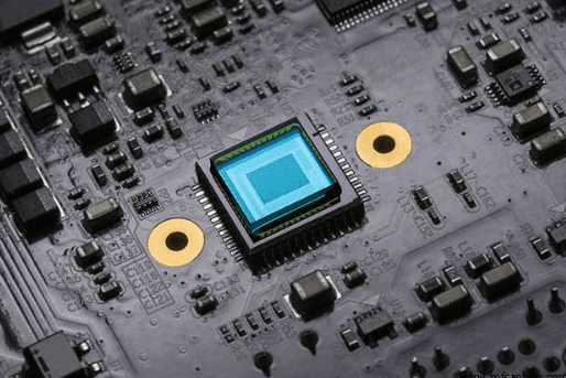
The structural design of optical PCB waveguides includes vertical coupling structures, where 45° end-face mirrors are key components. These end-faces are coated with reflective films to direct optical signals from the waveguide layer to photoelectric sensors, or vice versa. Research indicates that novel vertical coupling structure designs can significantly improve coupling efficiency while relaxing the requirements for precise optical-electrical alignment, making them more compatible with conventional PCB production processes.
Core Material Systems and Their Characteristics
Polymer materials are the preferred choice for optical PCB waveguides, primarily due to their processing flexibility and cost advantages. Commonly used polymer materials include:
- Polymethyl Methacrylate (PMMA): Refractive index ~1.48, good light transmittance, but heat deflection temperature is only 85°C, requiring copolymer modification to improve heat resistance.
- Polycarbonate (PC): Good heat resistance, capable of long-term use at 135°C, higher refractive index than PMMA, but poor UV resistance.
- Fluorinated Polyimide: A new high-performance waveguide material with a heat resistance temperature up to 380°C, near-infrared transmission loss ~0.3 dB/cm; refractive index can be controlled by adjusting the fluorine content.
- Organosiloxane Polymers: Can withstand 180°C and 15 kPa pressure, featuring low refractive index, low birefringence, and good thermal and humid stability.
To enhance material properties, researchers have developed various modification methods. For instance, introducing metal ions (e.g., Sn, Pb, Ba) into MMA copolymers can raise the glass transition temperature above 250°C; doping with nanoparticles (e.g., SiO₂, TiO₂) can significantly improve thermal stability and refractive index; and replacing hydrogen with heavy atoms like fluorine or chlorine can reduce optical propagation loss, increasing material transparency in the communication bands (1.3 μm and 1.55 μm).
Manufacturing Processes and Key Technologies
The manufacturing process for industrial sensor optical PCB waveguides primarily involves the following key steps:
- Alignment and Drilling: Utilizing the same drilling system to process multiple core boards, creating different types of alignment holes (e.g., panel edge, inner-panel, outline, pattern) to ensure alignment accuracy in subsequent processes.
- Inner Layer Patterning: Completing inner layer graphics processing through standard PCB processes like dry film lamination, exposure, development, and etching. For auxiliary core boards serving as optical waveguide substrates, the surface copper foil is entirely or partially etched away, leaving only the insulating substrate material.
- Optical Waveguide Line Processing: Sequentially coating the optical waveguide substrate board with a low-refractive-index lower cladding, a high-refractive-index core layer, and a low-refractive-index upper cladding. The core layer is patterned via UV lithography to form the waveguide pattern. This process can employ a CCD alignment system, using inner-panel alignment holes or copper pads as alignment targets.
- Lamination and Pressing: Embedding the processed optical waveguide substrate board into a pre-cut (hollowed-out) main core board, then laminating it in sequence with multiple prepreg sheets, followed by pressing. To improve accuracy, rivets can be placed in inner-panel and panel edge alignment holes for positioning.
Key manufacturing technologies also include laser direct writing, reactive ion etching, hot embossing, and electron beam writing. Among these, laser technology is particularly widely applied, capable of creating channels within polymer layers by laser ablation, defining optical interconnection schemes. Laser direct writing technology, which requires no mask, offers ease of achieving flexibility, high processing precision, high speed, and is pollution-free, making it a flexible wiring technology considered promising for industrial application.
Performance Advantages and Application Scenarios
Industrial sensor optical PCB waveguide technology offers multiple performance advantages:
- High Bandwidth and High-Speed Transmission: Optical interconnect technology holds an unparalleled advantage over electrical interconnects in terms of bandwidth-transmission distance product, supporting data rates of tens or even hundreds of Gbps, meeting the real-time data acquisition demands of industrial sensors.
- Strong Resistance to Electromagnetic Interference (EMI): Optical signal transmission is immune to EMI, making it particularly suitable for industrial sensor applications in high-EMI environments, such as power system monitoring and motor control.
- Low Power Consumption and Low Heat Generation: Optical transmission consumes significantly less energy than electrical transmission, helping to reduce the overall power consumption and cooling requirements of industrial sensor systems.
- High-Density Integration: Optical PCB waveguides enable efficient three-dimensional space utilization, significantly increasing interconnect density and supporting the trend towards miniaturization and integration in industrial sensors.
Application scenarios include high-speed data acquisition in industrial automation, industrial process control systems, robotic vision systems, and extreme environment monitoring. In industrial automation, optical PCB waveguide sensors are used to detect parameters like PCB position, dimensions, and defects, operating stably even in the presence of holes or grooves.
Technical Challenges and Development Trends
Industrial sensor optical PCB waveguide technology faces several technical challenges. Material compatibility is a key issue; waveguide materials must possess a coefficient of thermal expansion (CTE) matching that of the PCB substrate. Typically, epoxy-based systems have a Z-axis CTE in the range of 100-150 ppm, while the X and Y axes are around 16-18 ppm. Process consistency challenges cannot be ignored either; controlling process repeatability in mass production is difficult, and efficient coupling between waveguides and light sources/detectors requires precise alignment.
Future development trends include:
- New Material Development: Focusing on improving heat resistance and reducing transmission loss. New materials like fluorinated polyimide show broad application prospects.
- Hybrid Integration Technology: Promoting the combination of rigid and flexible optical waveguides to achieve optimal configurations for different sensor form factors. Flexible optical waveguide boards can be bent, coiled, and folded freely, arranged according to spatial layout requirements, and moved and stretched in three-dimensional space, making them suitable for high-speed connections in confined or moving parts.
- Manufacturing Process Innovation: Evolving towards finer and more efficient methods. For example, micro-pen writing is a novel direct-write fabrication technique that eliminates the need for pattern copying, photoplotting film, mask fabrication, etc. It directly writes waveguides onto various substrates using CNC machining data generated from CAD/CAM designs.
- Standardization and Cost Control: Promoting technological standardization, reducing manufacturing costs, and facilitating wider adoption. Currently, optical PCB waveguide manufacturing requires high-precision equipment and technical support, resulting in high costs that limit large-scale application.
Conclusion and Outlook
Industrial sensor optical PCB waveguide technology, as an interdisciplinary field, combines optoelectronics with innovations in traditional PCB manufacturing processes, opening new pathways for the development of industrial sensors. With advancements in materials science and micro/nano-fabrication technologies, this technology is expected to achieve further breakthroughs in performance enhancement, cost control, and application scope.
In the future, driven by the rapid development of fields such as the Industrial Internet of Things (IIoT), smart manufacturing, and autonomous driving, the demand for high-performance sensors will continue to grow. Optical PCB waveguide technology will play an increasingly important role. Technological innovation will propel industrial sensors towards higher integration levels, stronger anti-interference capabilities, and broader application scenarios, providing key technical support for Industry 4.0 and digital transformation.
Concurrently, rigid and flexible optical waveguides will develop synergistically based on application needs – rigid optical waveguides ensure reliable optical signal transmission in harsh industrial environments due to their good mechanical stability, while flexible optical waveguides are suited for complex spatial layouts and movable components, collectively advancing industrial sensor technology.


0 Comments