
Introduction: The Cornerstone of Power Conversion
In the era of pursuing green energy, inverters, as critical devices for converting Direct Current (DC) to Alternating Current (AC), have become indispensable components in clean energy systems such as solar photovoltaics and wind power. The inverter PCB (Printed Circuit Board) serves as the “skeleton” and “nerve center” of the inverter, bearing the critical responsibilities of power transmission, signal control, and system coordination. Whether in small household solar systems or megawatt-scale photovoltaic power plants, the design and manufacturing quality of the inverter PCB directly determine the efficiency, stability, and reliability of power conversion. This article provides an in-depth analysis of the working principles, design challenges, key technologies, and future development trends of inverter PCBs, revealing how this “unsung hero” drives the green energy transformation.
Basic Working Principles of Inverter PCBs
The core function of an inverter PCB is to accomplish the conversion from DC to AC, a process primarily divided into two key stages.
First, the DC-DC boost stage elevates the low-voltage DC (e.g., 12V, 48V) from batteries or solar panels to a higher DC voltage (e.g., 370V-380V). This process typically employs push-pull or full-bridge circuits, utilizing high-frequency switching control of power switching devices (such as MOSFETs, IGBTs) in conjunction with the electromagnetic induction of high-frequency transformers to achieve voltage boosting.
Second, the DC-AC inversion stage converts the high-voltage DC into AC via an H-bridge circuit. Using Sinusoidal Pulse Width Modulation (SPWM) technology, it generates high-frequency AC that simulates a sine wave by controlling the switching sequence of the power switching devices. This high-frequency AC is then processed through an LC filter circuit to output a pure sine wave AC, whose waveform quality is far superior to that of square wave or modified sine wave inverters.
The core of the entire control system is a microcontroller (such as the TDS2285 chip) or Digital Signal Processor (DSP), which is responsible for generating precise PWM signals and monitoring system status in real-time to ensure stable inverter operation.
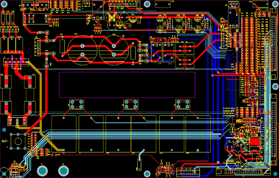
Key Components of an Inverter PCB
A complete inverter PCB system typically comprises multiple functional modules, each assigned specific tasks:
- Power Mainboard: The core of the inverter, containing the two main power conversion sections: DC-DC push-pull boost and H-bridge inversion. Key components include high-power transistors (e.g., 190N08, IRFP460), high-frequency transformers, and fast-recovery diodes (e.g., RHRP8120), which handle high voltage and high current.
- SPWM Driver Board: Utilizes a microcontroller chip (e.g., TDS2285) to generate precise SPWM signals, driving the power switching devices of the H-bridge via optocoupler isolation. To ensure driving reliability, a bootstrap circuit is often required to stabilize the driving voltage at 12-15V.
- DC-DC Driver Board: Based on a PWM control chip (e.g., SG3525), it generates high-frequency switching signals to control the operation of the front-stage boost circuit. This section determines the efficiency and stability of the boost conversion.
- Protection Circuitry: Implements multiple protection functions such as over-voltage, under-voltage, over-current, and over-temperature, ensuring the system shuts down safely under abnormal conditions and prevents equipment damage.
Furthermore, filter circuits (e.g., AC output filter ferrite cores) are crucial for output waveform quality, while thermal management systems (e.g., heat sinks, fans) are key to maintaining stability during high-power operation.
Design Challenges and Special Requirements for Inverter PCBs
Inverter PCB design faces multiple severe challenges, especially in high-power and harsh environment applications.
- High Voltage and High Current Carrying Capacity is a primary challenge. New energy inverters (particularly 1500V photovoltaic systems) need to handle peak currents exceeding 100A, which is challenging for standard PCB designs. Solutions include using 4oz (140μm) heavy copper foil, controlling current density within 8A/mm², and designing the main current path as multiple parallel traces to distribute current and reduce local hotspots.
- Thermal Management is a critical factor affecting reliability. Heat generated during inverter operation, if not dissipated promptly, can cause component temperatures to soar, leading to performance degradation or damage. Optimization measures include: using an “FR-4 + Aluminum substrate” composite structure under IGBTs; arranging dense arrays of thermal vias (aperture 0.4mm, pitch 1mm); and designing “copper foil heat dissipation grids” around heat-generating components to Increase the heat dissipation area (Note: English term used earlier is ‘heat dissipation area’).
- Electromagnetic Compatibility (EMC) design is equally crucial. High-frequency switching operations generate significant electromagnetic interference, which can affect the accuracy of control signals. Superior designs employ differential pair routing (trace width 0.2mm, spacing 0.15mm, impedance 100Ω ±3%) for critical synchronous signals; setting up “ground isolation moats” around sensitive lines; and placing ferrite beads in series and capacitors in parallel at signal inputs to filter out noise.
- Environmental Adaptability cannot be overlooked. Inverter PCBs for outdoor applications must withstand harsh conditions like temperature variations (-30°C to 70°C), humidity, and dust. Protective measures include: using epoxy potting compound for core areas (potting thickness ≥3mm, IP67 waterproof rating); implementing “stainless steel edging + silicone waterproof sealant filling” along PCB edges; and utilizing professional waterproof connectors.
Material Selection and Process Considerations
The performance of an inverter PCB largely depends on material selection and manufacturing processes.
- Substrate Materials: Common choices include:
- FR-4: A versatile material with good mechanical strength and electrical properties, cost-effective, suitable for most inverter applications.
- Metal Core Substrates: Such as aluminum substrates, offering excellent thermal conductivity, suitable for high power density designs, enabling rapid heat transfer from power components to heat sinks.
- Polyimide and PTFE: Suitable for high-temperature and high-frequency applications, but at a higher cost.
- Conductive Materials: Copper foil is typically chosen, with its thickness determined by current levels. High-current paths (main loops) require thickened copper foil (2-4oz), or even the use of busbar bonding technology, where copper busbars are soldered directly onto the PCB surface, significantly enhancing current-carrying capacity and improving heat dissipation.
- Manufacturing Processes: High-reliability inverter PCBs require: strict control of trace width and spacing to ensure signal integrity; use of blind and buried vias to increase routing density; and application of surface finishes (such as ENIG, HASL) to enhance solderability and corrosion resistance.
- Thermal Management Processes: Beyond optimizing substrate selection, it is also necessary to distribute heat-generating components evenly in the layout to avoid hot spots; using thermal paste between high-power components and the PCB to fill gaps and reduce thermal resistance.
Classification and Application Scenarios of Inverter PCBs
Inverter PCBs can be classified based on various criteria:
- By Output Waveform:
- Square Wave Inverter PCB: Simple structure, low cost, but high harmonic content, only suitable for resistive loads with low power quality requirements.
- Modified Sine Wave Inverter PCB: Improved waveform, reduced harmonics, can power most common appliances.
- Pure Sine Wave Inverter PCB: Output waveform closely approximates a perfect sine wave, low harmonic distortion, suitable for sensitive electronic equipment like medical devices, air conditioners, computers.
- By Application Scenario:
- Grid-Tie Inverter PCB: Converts DC from solar power into AC synchronized with the grid, enabling feed-in of surplus power. Designs require high-precision synchronization (frequency deviation ≤ ±0.5Hz) to ensure grid safety.
- Off-Grid Inverter PCB: Used in standalone systems not connected to the grid, typically paired with batteries.
- Hybrid Inverter PCB: Combines both grid-tie and off-grid functionalities, capable of managing energy flow between PV arrays, the grid, and battery storage.
- By Power Rating:
- Low Power PCB (<1kW): For small household systems or portable devices.
- Medium Power PCB (1-10kW): Suitable for residential and small-to-medium commercial premises.
- High Power PCB (10-100kW) and Ultra-High Power PCB (>100kW): For large commercial and industrial facilities.
Common Failures and Solutions
Failures in inverter PCBs can stem from various factors. Understanding these aids in designing more reliable products.
- Overheating Failures are among the most common issues. During high-power operation, insufficient thermal design can lead to excessive component temperatures, performance degradation, or permanent damage. Solutions include: optimizing heat dissipation paths, using heat sinks + fans for active cooling; ensuring adequate spacing between power components during PCB layout to prevent heat concentration; employing temperature sensors for real-time monitoring to trigger over-temperature protection.
- Failures due to Environmental Factors are also significant. Inverter PCBs in outdoor applications are susceptible to moisture, dust, and salt spray corrosion, leading to reduced insulation, short circuits, etc. Protective measures include: applying conformal coating over the entire board; using epoxy resin potting for critical areas; selecting connectors with high ingress protection (IP) ratings.
- Manufacturing Defects can also cause failures, such as cold solder joints, copper foil burrs causing shorts, or substandard material quality. Quality control methods include: Automated Optical Inspection (AOI) during production; rigorous electrical performance testing of finished products; performing withstand voltage tests (e.g., 1500V insulation strength test) on high-voltage sections.
Proactive and corrective measures for these issues include: regular dust removal to maintain clear cooling systems; enhancing moisture protection in humid environments; selecting reliable quality components and PCB manufacturers.
Future Development Trends and Outlook
Inverter PCB technology is rapidly evolving towards higher efficiency, greater intelligence, and deeper integration.
- Enhanced Efficiency is a perpetual pursuit. By adopting new wide-bandgap semiconductor materials (such as Silicon Carbide and Gallium Nitride), inverter switching frequencies can be significantly increased while reducing losses and physical size. Optimizing circuit topologies and control algorithms (like Maximum Power Point Tracking algorithms) can also markedly improve conversion efficiency.
- Intelligence is a key development direction. Future inverter PCBs will integrate more sensors and microprocessors to enable self-status monitoring, fault diagnosis, and predictive maintenance. Through data analysis and machine learning algorithms, inverters can automatically optimize operating parameters to increase energy yield.
- Integrated PV-Storage-Charging is becoming a leading trend. Inverter PCBs will no longer be confined to a single power conversion function but will act as the core of integrated systems, simultaneously managing solar PV generation, battery storage, and electric vehicle charging, achieving optimal energy configuration and utilization.
- Modular Design enhances system flexibility. By decomposing inverter functions into independent modules, hot-swappable maintenance is enabled, simplifying the fault repair process. Modular design also facilitates system capacity expansion based on demand, lowering the initial investment threshold.
With the continuous application of new materials, processes, and smart technologies, inverter PCBs will continue to play the role of the “unsung hero” in the green energy transition, providing a solid technical foundation for building a sustainable energy future.


0 Comments