
Introduction to the 48-Port Switch PCB
The 48-port switch PCB serves as the fundamental platform for high-density network switching, integrating complex circuitry to enable seamless data transmission across all ports. As port densities and data rates increase, the design and layout of the 48-port switch PCB become increasingly critical, directly determining signal integrity, power stability, and thermal performance. This article provides a detailed analysis of the 48-port switch PCB, examining its structural composition, key design challenges, and specialized solutions for industrial-grade applications.
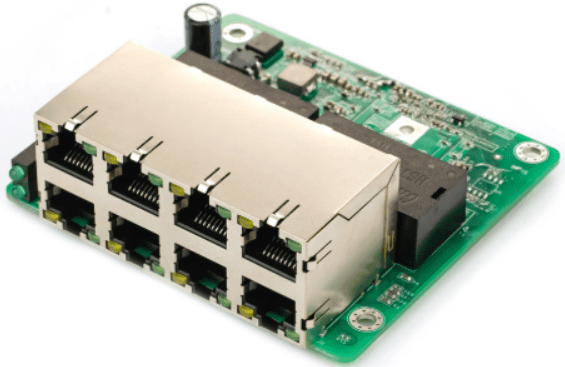
The primary function of the 48-port switch PCB is to provide the physical interconnection platform for 48 Gigabit Ethernet ports and their associated interface circuits. These ports must support high-speed data switching and may also incorporate functional units such as 10-Gigabit uplinks and management modules. Under such high-density port configuration, the PCB must coordinate the layout, routing, and signal integrity for hundreds of components, ranging from interface magnetics and PHY chips to the switch fabric ASIC and clock circuits [sitation:1].
Compared to standard commercial switches, industrial-grade 48-port switches entail more complex PCB designs, necessitating enhanced protective measures and specialized processing techniques. For instance, industrial-grade switch PCBs often employ Immersion Gold (ENIG) surface finish. Gold’s stable chemical properties and dense crystalline structure resist oxidation, significantly extending product lifespan. Additionally, these PCBs require Conformal Coating (protection against moisture, fungus, and dust) to withstand harsh operating environments.
With the rapid evolution of data centers, per-lane signal rates in switches have escalated dramatically, from early 1Gbps to current 56Gbps and beyond, posing new challenges for PCB design and Signal Integrity (SI). An exemplary 48-port switch PCB design demands comprehensive optimization across material selection, stack-up architecture, routing strategies, and manufacturing processes to meet the stringent requirements of high-performance network equipment for bandwidth, latency, and reliability.
Design Challenges and Key Performance Indicators
The PCB design for a 48-port network switch confronts three primary challenges: High-Speed Signal Integrity, Power Integrity, and Thermal Management. These challenges directly impact switch performance and reliability, requiring dedicated design strategies for mitigation.
- High-Speed Signal Integrity Challenge: As per-lane signal rates reach 56Gbps, PCB transmission loss becomes a critical issue. Solutions include selecting low-loss materials (e.g., Hyper Low Loss laminates, controlling loss to within -0.66dB @12.89GHz), implementing rational stack-up design to ensure the shortest signal return paths, and designing complete isolation between Serdes TX and RX signals to prevent crosstalk.
- Power Integrity Challenge: High-density 48-port switches involve multiple voltage domains and complex power distribution. Mitigation strategies involve isolating power planes from signal layers using GND planes, implementing multi-stage decoupling strategies, and optimizing the Power Delivery Network (PDN) impedance.
- Thermal Management Challenge: Operation with all 48 ports under full load generates significant heat. Industrial-grade designs ensure effective heat dissipation through large copper pours, thermal vias, heatsinks, and Conformal Coating processes. The conformal coating forms a protective film that effectively isolates the board, safeguarding circuits from harsh environmental factors, thereby enhancing reliability.
Table: Key Design Indicators for 48-Port Switch PCBs (Example)
| Indicator Category | Specific Parameter | Industrial-Grade Requirement |
|---|---|---|
| Signal Integrity | Differential Impedance Control | 100Ω ±10% |
| Power Integrity | Voltage Ripple | ≤ 5% |
| Protection Rating | IP Rating | IP40 or higher |
| Environmental Suitability | Operating Temperature Range | -40°C to +85°C (Industrial) |
Critical Components and Layout Techniques
The PCB layout of 48-port network switch is a very complicated system engineering., requiring careful consideration of the interrelationships between functional modules and their impact on overall performance. A rational layout optimizes signal integrity, enhances power distribution efficiency, and alleviates thermal management pressure.
The Switch ASIC, acting as the switch’s “brain,” requires critical placement consideration. It is typically positioned near the center of the PCB to minimize differences in signal path lengths to various ports. DDR memory and Flash components should be placed closely around the switch ASIC, adjacent to their corresponding interfaces, to reduce signal reflection and timing issues. Given the numerous PHY chips required for 48 ports (typically twelve 4-port Gigabit Ethernet PHY chips), they must be distributed evenly around the switch ASIC.
The Port Module layout must strictly follow the signal flow. RJ45 connectors should be arranged along the board edge for easy interface routing and chassis installation. The network transformers must be placed immediately adjacent to the RJ45 connectors (distance typically controlled within 1000 mils), and the PHY chips should, in turn, be adjacent to the transformers. This sequential layout (RJ45 → Transformer → PHY) ensures minimized and linearized signal paths. Integrated Transformer RJ45 connectors can simplify the layout but still require maintaining coherent signal flow.
The Clock Circuitry is crucial for data synchronization. A 48-port switch requires numerous reference clocks, often implemented using a cost-effective crystal oscillator plus clock buffer solution. Clock circuits must be placed away from board edges, interfaces, and other high-frequency components, and shielded by ground planes to mitigate external interference. Solutions like Silicon Labs’ Si51x series oscillators with SI533xx clock buffers can provide low-jitter clock sources for multiple PHY interfaces.
The Power Management Module layout must consider power transmission efficiency and thermal distribution. DC-DC converters should be placed close to high-power consumption devices (e.g., the switch ASIC), while LDO regulators can power local circuits. Filter capacitors, particularly high-frequency decoupling capacitors, should be distributed uniformly around power modules and placed as close as possible to the chips’ power pins.
[Flowchart: 48-Port Switch PCB Layout Logic]
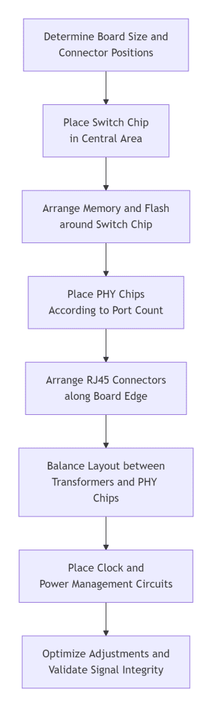
For a 48-port switch PCB, Module Partitioning is fundamental for effectively managing high-density routing. The board can typically be divided into zones: Switch ASIC area, PHY chip area, Port connection area, Power area, and Clock area. Each functional zone should have clear boundaries to avoid crossover. Digital, analog, and power circuits should be isolated from each other, and ground plane segmentation must be carefully planned to reduce noise coupling.
Furthermore, LED indicator driver circuits should avoid high-speed differential lines, be isolated by a ground plane where space permits, and have minimized loop areas. The Bob Smith Termination circuit (comprising 75Ω resistors) must be placed close to the network transformers with short, thick traces; this circuit effectively filters common-mode noise, reducing EMI by approximately 10dB.
High-Speed Signal Integrity Design
In 48-port network switch PCB design, high-speed signal integrity is paramount for ensuring reliable data transmission. With numerous concurrent high-speed data streams, any signal quality issue can lead to bit errors, packet loss, or even link failure, necessitating a systematic signal integrity control strategy.
Differential Pair Control is the cornerstone of Ethernet PCB design. Gigabit Ethernet involves multiple differential pairs (two pairs for Fast Ethernet, four pairs for Gigabit Ethernet). These differential pairs (Rx±, Tx±) must maintain strict length matching and consistent spacing. Routing should adhere to the “parallel, equal-length, short-distance” principle, avoiding vias and crosses whenever possible. For 48-port switches, the length matching tolerance for differential pairs is typically controlled within 5 mils (approx. 0.127 mm) to minimize timing skew and common-mode interference. Achieving this requires precise serpentine trace routing for length compensation, maintaining consistent trace width and spacing while avoiding sharp bends and right-angle turns.
Impedance Matching is another critical factor for signal integrity. Differential signals on the secondary side of the network transformer require strict impedance control, typically targeting 100Ω ±10%. Achieving this necessitates precise calculation of trace parameters: for outer-layer microstrip lines, a design with 0.5-oz copper thickness plus plating might be used; for inner-layer stripline, 1-oz copper thickness is common. Impedance control involves not only trace width and spacing but also dielectric thickness and permittivity, requiring close collaboration with the PCB manufacturer to determine the appropriate stack-up.
Termination Strategy is crucial for preventing signal reflections. Proper termination absorbs signal energy, reducing distortion from reflections. In Ethernet design, the Bob Smith circuit is a specific termination technique providing common-mode termination using 75Ω resistors and capacitors. This circuit must be placed close to the network transformer with short, thick traces to minimize parasitic inductance.
For 56Gbps and higher-speed signals, more advanced signal integrity techniques are required. 10-Degree Angle Routing helps mitigate impedance discontinuities caused by the fiberglass weave effect. Via-in-Pad design optimizes impedance continuity in areas like the switch ASIC and optical module connectors. Antipad Optimization adjusts the antipad size around vias to fine-tune the capacitive characteristics of the via impedance. Furthermore, 3D Back-Drilling technology can precisely control the via stub to within 2-8 mils, significantly improving signal reflection issues.
Table: High-Speed Signal Key Parameter Requirements for 48-Port Switches
| Signal Type | Impedance Requirement | Length Matching Requirement | Spacing Requirement |
|---|---|---|---|
| Gigabit Ethernet Diff Pair | 100Ω ±10% | ≤ 5 mils | ≥ 4W (W = Trace Width) |
| Serdes High-Speed Signal | 85Ω ±8% | ≤ 2 mils | ≥ 3W |
| Clock Signal | Diff: 100Ω ±5%, SE: 50Ω ±5% | ≤ 1 mil | Reference Plane Isolation |
Grounding Strategy significantly impacts signal integrity. The area beneath network transformers should implement Ground Plane Segmentation, creating an isolation zone (typically >100 mils) to prevent noise coupling. RJ45 connectors and the transformer secondary side should use a separate, isolated ground, connected to the main board ground via capacitors or resistors at the transformer’s center tap. This split grounding strategy ensures good common-mode noise rejection while providing an effective electrical isolation barrier.
For high-density boards like 48-port switches, Crosstalk Control cannot be overlooked. High-speed signal lines must maintain sufficient spacing (at least 3 times the trace width), adding guard traces if necessary. Different signal groups should be isolated by ground planes, avoiding long parallel runs. For particularly sensitive signals, a stripline structure can be used instead of microstrip to leverage the shielding effect of the upper and lower ground planes.
PCB Materials and Advanced Manufacturing Processes
The performance of a 48-port network switch is highly dependent on PCB material selection and manufacturing processes. As signal rates advance to 56Gbps levels, standard FR-4 materials struggle to meet low-loss demands, necessitating advanced high-speed laminates and precision fabrication techniques.
The selection of High-Speed Laminates is fundamental for ensuring signal transmission quality. For 56G signals, Hyper Low Loss grade materials are recommended, with loss controlled within -0.66dB @12.89GHz. These materials typically feature lower Dielectric Constant (Dk) and Dissipation Factor (Df), significantly reducing signal attenuation. Common high-speed laminates include brands like Rogers, Taconic, and Nelco, alongside some domestic high-end alternatives. Material selection requires a balanced consideration of electrical performance, processability, thermal reliability, and cost.
Immersion Gold (ENIG) Surface Finish is a common choice for industrial-grade switch PCBs. Gold’s stable chemical nature and dense structure resist oxidation, enhancing product lifespan. Compared to traditional HASL or OSP finishes, the ENIG surface is flatter, beneficial for fine-pitch component soldering and providing better contact reliability. For high-density boards like 48-port switches, ENIG also ensures reliable soldering quality for BGA-packaged chips, reducing soldering defects.
Conformal Coating is a hallmark process for industrial-grade switches. The coating forms a protective film on the PCB surface, effectively isolating the board from harsh environments and protecting circuits from moisture, dust, and chemical contaminants. This not only improves board reliability but also, by preventing leakage currents and short circuits, allows for higher power density and closer board spacing, thereby supporting component miniaturization. In industrial settings, where dust accumulation combined with humidity can cause short circuits, conformal coating fundamentally mitigates this risk.
High-Density Interconnect (HDI) technology is crucial for 48-port switch PCBs. As signal rates increase and board sizes are constrained, traditional through-hole vias become insufficient. Skip Via technology uses controlled-depth drilling followed by laser drilling to connect outer layers to the third layer, ensuring signal connectivity without creating stubs, thereby greatly enhancing signal integrity. Compared to blind vias, the Skip Via process has a shorter cycle time (no multiple lamination cycles) and is simpler, offering significant cost advantages.
Resin Plugging is a key process for enhancing PCB reliability. It is recommended that all 8-10 mil vias utilize resin plugging, a vacuum filling process that ensures 100% resin fill within the via. Compared to standard solder mask plugging, resin plugging does not trap air or moisture, fundamentally preventing via barrel corrosion from moisture, enhancing long-term via reliability, and extending board service life.
POFV (Plated Over Filled Via), also known as Via-in-Pad, technology is specifically designed for 56G Serdes transceiver interfaces. This technique places the signal layer transition via directly within the component’s solder pad, saving PCB layout space while significantly improving SI and PI performance. During manufacturing, the via is drilled, plated, filled with resin, and then plated over to create a flat surface suitable for SMD component attachment.
Precision Lamination technology is critical for layer-to-layer registration in multilayer PCBs. Techniques like PIN Lamination combined with CCD Electromagnetic Fusion are recommended to maximize lamination alignment accuracy, controlling layer-to-layer misregistration to within 3 mils and overall misregistration within 5 mils. This is vital for high-layer-count (often 12+ layers), high-density boards like 48-port switches, ensuring the continuity and consistency of impedance control.
Industrial-Grade Enhanced Design
Industrial-grade 48-port network switch PCBs differ significantly from their commercial counterparts, as they must endure harsher operating environments, including extreme temperatures, humidity, vibration, and electromagnetic interference. Consequently, industrial-grade switch PCBs incorporate a series of enhanced design measures to ensure stable operation under demanding conditions.
Water and Dust Ingress Protection is a primary concern for industrial-grade switches. The IP (Ingress Protection) rating system defines their防护 capability. For example, an IP45-rated industrial switch can prevent the ingress of solids larger than 1mm and remain stable operating under water jet spray. Industrial switches typically require at least an IP40 rating, with products for particularly harsh environments demanding ratings up to IP67. This protection is achieved through sealed enclosures, gaskets, and PCB conformal coating.
Shock and Vibration Resistance addresses physical stresses in industrial environments. In applications like mining and rail transportation, equipment faces impacts and drops. Industrial-grade switches protect internal components against strong physical shocks by using reinforced PCB substrates, optimizing mounting point designs, and employing shock-resistant components. The IEC (International Electrotechnical Commission) sets a series of shock and vibration test standards that industrial switch PCB designs must comply with, ensuring connections remain secure and components intact under vibration.
Wide Temperature Operation is a key characteristic of industrial-grade PCBs. Unlike commercial products rated for 0°C to 70°C, industrial switches typically need to support -40°C to +85°C or wider ranges. This requires selecting components rated for industrial temperature ranges and optimizing thermal design. For low temperatures, matching coefficients of thermal expansion (CTE) of materials is crucial to prevent cracking; for high temperatures, materials must have a sufficiently high Glass Transition Temperature (Tg), typically selecting high-Tg materials (Tg ≥ 170°C).
Electromagnetic Compatibility (EMC) design is vital for industrial settings, which contain numerous strong interference sources like motors and frequency converters. Industrial switches require robust EMC performance, often needing to meet Level 4 EMC standards and 4000V surge protection for lightning. PCB design strategies include optimized grounding, enhanced filtering on circuits, and effective surge protection measures on interfaces. Protection components like varistors and TVS diodes are typically added at power inputs, with appropriate filtering on data lines.
Reliability and Maintainability design are core values of industrial-grade switches. Network failures in industrial production can lead to significant economic losses or safety incidents; therefore, industrial networks must possess high reliability, recoverability, and maintainability. PCB designs should incorporate comprehensive diagnostic and monitoring circuits (e.g., for voltage, current, temperature) to facilitate predictive maintenance. For critical applications, redundant power supplies or circuit paths may be necessary.
Real-Time Performance Guarantee is especially critical for industrial control systems. Industrial environments impose strict requirements on data transmission determinism, often requiring data updates within tens of milliseconds. Industrial switch PCB design must minimize signal transmission latency and optimize signal paths to avoid uncertainties caused by retransmission mechanisms. Industrial Ethernet switches utilize store-and-forward switching with intelligent alarm systems to monitor network health, ensuring reliable and stable Ethernet operation even in harsh industrial environments.
Compared to “Industrial-Tolerant” products, genuine industrial-grade switch PCBs adhere to strict standards and design considerations regarding dust protection, EMI, and temperature tolerance, areas where industrial-tolerant products often show significant shortcomings, making them unsuitable for long-term stable operation in true industrial settings. Therefore, when selecting switches for industrial applications, careful scrutiny of their PCB design standards and process levels is essential to ensure they meet the specific environmental requirements.
Summary and Outlook
The PCB design for a 48-port network switch is a complex, multidisciplinary endeavor involving high-speed digital circuits, RF/microwave techniques, thermodynamics, and materials science. An excellent PCB design achieves the optimal balance between performance, cost, and reliability, meeting the demanding requirements of modern network equipment for high bandwidth, low latency, and high availability.
With advancing technology, 48-port switch PCB design faces new trends and challenges. Signal rates continue to climb from 56G towards 112G and beyond, demanding PCB materials with superior loss characteristics. System integration density is increasing, with switch ASICs incorporating more ports and complex functionalities, requiring PCB designs to support higher interconnect densities. Thermal management needs are becoming more prominent with rising power density, driving the adoption of more efficient cooling solutions like metal core PCBs and embedded heat pipes.
In the industrial sector, the rapid development of the Industrial Internet of Things (IIoT) presents new opportunities and challenges for industrial-grade switch PCBs. Applications in smart grids, intelligent transportation, and industrial automation are deepening, requiring industrial switches with greater environmental resilience, stricter real-time performance, and higher reliability. Future industrial switch PCBs may integrate more intelligent monitoring functions (e.g., for temperature, vibration, corrosion) and AI-based predictive maintenance capabilities.
Environmental Sustainability is also becoming a significant consideration in PCB design. Eco-friendly processes like halogen-free laminates and lead-free surface finishes will see wider adoption, alongside recyclable designs aligned with circular economy principles. Energy consumption control and waste management during PCB manufacturing are also becoming factors designers must consider.
In summary, 48-port network switch PCB design is a continuously evolving field, requiring designers to constantly acquire new knowledge and master emerging technologies to maintain a competitive edge. Whether for commercial or industrial applications, superior PCB design remains the cornerstone of a successful switch product, warranting substantial resources and effort for in-depth research and optimization.


0 Comments