
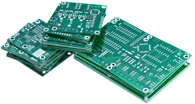
In the vast world of electronics creation, the Printed Circuit Board (PCB) is the core medium that transforms abstract circuit diagrams into physical reality. When the limited routing space of a single-sided board becomes restrictive, the double sided PCB naturally emerges as the upgrade of choice. It acts like a dual-sided stage for circuits, significantly enhancing routing flexibility and complexity. But how can one use it to maximize its potential and avoid common pitfalls?
What is a Double Sided PCB Board?
As the name suggests, a double sided PCB is a board with copper foil on both the Top Layer and the Bottom Layer of the substrate, allowing the two layers to be electrically connected through Vias.
- Top and Bottom Layers: Typically used for placing components and routing traces.
- Vias: These are the soul of the double-sided board. They are small holes drilled into the board and metallized (usually plated), creating conductive bridges between the top and bottom layers.
Why Choose a Double Sided PCB Board?
Compared to single-sided boards, double-sided boards offer significant advantages:
- Higher Routing Density: You can utilize the space on two layers for routing, easily navigating around crossing traces and solving the common “jumper wire” problem of single-sided boards.
- Better Signal Integrity: Allows for providing a continuous ground shield for sensitive signals (like clock signals).
- More Compact Design: Enables the creation of smaller, more refined circuit boards.
- Better Suited for Complex Circuits: Ideal for modern microcontroller, digital IC, and mixed-signal circuit projects.
Double Sided PCB Materials and Structure
When learning how double-sided PCBs work, understanding their construction materials is crucial. A typical PCB includes the following parts:
- Substrate Layer (FR-4 or CEM-1): Insulating base material.
- Copper Layer: Located on each side, used for transmitting signals.
- Solder Mask Layer: Covers the copper traces except for areas that need soldering.
- Silkscreen Layer: The text and symbols on the board are printed using this layer.
- Vias: Plated mechanical holes used to connect the two sides.
Complete Workflow for Using a Double Sided PCB Board
Step 1: Design – Creating the Blueprint in the Virtual World
This is the most critical step, determining the success or failure of the final product.
- Choose Design Software: Use professional EDA (Electronic Design Automation) software like KiCad (free, open-source), Eagle (now part of Fusion 360), or Altium Designer (professional grade).
- Schematic Capture: Draw your circuit schematic correctly, ensuring every component has a corresponding footprint.
- PCB Layout:
- Define Board Outline: First, determine the shape and size of the circuit board.
- Component Placement: This is a blend of art and science. Place key components (like the MCU, crystal oscillator) centrally, with related components arranged around them. Consider heat dissipation, signal flow, and mechanical structure.
- Routing:
- Prioritize Power and Ground Traces: Power and ground traces often require wider widths to carry higher currents.
- Utilize Both Layers: A common strategy is to route primarily horizontal traces on the top layer and vertical traces on the bottom layer (or vice versa), which can effectively reduce inter-layer interference.
- Use Vias Wisely: When a trace cannot be completed on one layer, use a via to “jump” it to the other layer. In software, via placement is often automatic or semi-automatic.
- Create a Ground Plane: If space allows, dedicating a large portion of the bottom layer’s copper as a ground (GND) plane is an excellent practice. This provides a stable reference ground, reduces noise, and improves EMC (Electromagnetic Compatibility).
- Design Rule Check (DRC): Before sending the design for manufacturing, always run the DRC. The software will automatically check if clearances, trace widths, via sizes, etc., meet your (or the PCB manufacturer’s) process requirements.
Step 2: Manufacturing – Turning the Blueprint into Reality
For hobbyists, there are two main approaches:
- Outsourcing to a Professional PCB Fab House (Recommended): This is currently the most mainstream and quality-assured method. Send your design files (usually Gerber files and drill files) to a fab house. They can produce high-precision, high-quality double-sided boards with plated through-hole vias at very affordable prices.
- Handmade Fabrication (Suitable for urgent, simple prototypes):
- Transfer/Photosensitive Method: Create the circuit pattern on both sides of the board separately.
- Drilling: Use a mini drill press to drill holes for all pad and via locations.
- Via Connection (The Challenge): This is the biggest challenge in making double-sided boards by hand. Methods include:
- Wire Method: Thread a thin copper wire through the hole, solder it on both sides, and trim the ends.
- Copper Rivets: Use specialized copper rivets inserted into the vias.
- Conductive Silver Paste: Inject conductive silver paste into the vias, but its resistance and reliability are inferior to plated holes.
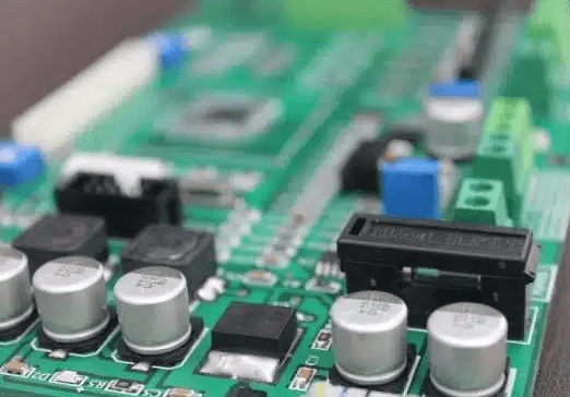
Step 3: Soldering – Bringing the Circuit to Life
Soldering double-sided boards requires more patience and skill.
- Prepare Tools: A good temperature-controlled soldering iron, thin gauge solder wire, flux, desoldering braid, and a magnifying glass.
- Soldering Sequence: Follow the “shortest first” principle. Solder shorter components like resistors and IC sockets first, then taller components like capacitors and connectors.
- Soldering Through-Hole Pins: For component pins that connect both sides (like headers, through-hole resistors), ensure the solder forms a full fillet on both the top and bottom layers. This guarantees a reliable connection for the pin between the two layers.
- Check for Bridges and Cold Joints: After soldering, carefully inspect for solder bridges between adjacent pins, especially on chips and connectors. Use a magnifying glass for assistance.
Step 4: Testing and Debugging – Ensuring Everything is Perfect
- Visual Inspection: Confirm again that all components are soldered correctly, with no shorts or open circuits.
- Continuity Test:
- Multimeter Test: Use the multimeter’s continuity or resistance mode to check for shorts between power and ground (this is the first step!).
- Refer to Schematic: Check if key nets (like power, important signal lines) are connected correctly, especially the reliability of via connections. Place one probe on a pad on the top layer and the other on the corresponding via or pad on the bottom layer to confirm connectivity.
- Power-On Test: Only apply power after confirming no shorts. It’s advisable to use an adjustable current-limited power supply. Set a lower voltage and a low current limit initially, observe if the board’s current draw is normal, and then gradually adjust to the normal operating voltage if no abnormalities are detected.
Advanced Double Sided PCB Design and Layout Strategies
- Layer Concept and Planning
- Signal Layer vs. Power Layer: In complex double-sided designs, a very classic and effective strategy is to use one layer primarily as a signal layer (for routing various signal traces) and the other primarily as a power/ground plane. Often, the bottom layer is used as a full or large-area ground plane.
- The Magic of a Ground Plane:
- Provides a Stable Reference Ground: Offers a low-impedance return path for all signals.
- Shielding and Noise Reduction: Effectively suppresses Electromagnetic Interference (EMI) and reduces crosstalk between signals.
- Improves EMC: Helps the product pass Electromagnetic Compatibility tests.
- Types of Vias and Their Applications
Beyond the basic vias connecting two layers, there are several special types:- Through-Hole Via: A via that goes from the top layer all the way through to the bottom layer; the most common type.
- Blind Via: Connects an outer layer to an inner layer (in multi-layer boards) but does not go through the entire board.
- Buried Via: Connects two or more inner layers and is not visible from the surface.
- Stamp Hole: Often used for board-to-board connections, like between a microcontroller core board and a carrier board.
- Note: Blind and buried vias are primarily used in high-end PCBs with four or more layers; double-sided boards typically only use through-hole vias.
- Routing Techniques for Critical Signal Lines
- Crystal Oscillator Circuit: The crystal and its load capacitors should be placed as close as possible to the chip’s clock pins. There should be a solid ground plane underneath it, and it should be surrounded by ground vias for “shielding.” Keep traces short and straight.
- Differential Pairs: Such as USB, CAN bus. The two traces need to be routed with equal length, equal spacing, and parallel to each other to achieve good common-mode rejection.
- High-Frequency Signals: Traces should be short and thick. Avoid 90-degree angles (use 45-degree angles or rounded corners) to reduce signal reflection and radiation.
- Power Handling
- Star Connection: Power for analog and digital sections should be routed separately from the main power entry point, like rays from a star, to prevent noise from the digital section from coupling into the analog section via the power lines.
- Power Trace Width: Calculate the required trace width based on current. A simple rule of thumb is: 1A current requires at least 1mm (40mil) trace width (refer to the PCB manufacturer’s current capacity chart for specifics).
- Decoupling Capacitor Placement: This is crucial. Place a decoupling capacitor (typically 0.1µF) as close as possible between the power and ground pins of each integrated circuit (IC). Its vias should connect directly to the power and ground planes to form the smallest current loop.
Deep Dive: Double Sided PCB Manufacturing Process
Understanding the fab house’s process flow helps you design boards that are easier to manufacture and have higher yield.
- Electroless Copper Deposition & Plating: This is the core process for creating electrical connections in vias. After drilling holes, a thin layer of copper is chemically deposited onto the non-conductive hole walls (electroless copper deposition), followed by electroplating to thicken this layer, ensuring reliable conductivity.
- Solder Mask: That green (or other colored) coating. It covers the copper foil, preventing bridges during soldering and protecting the traces from oxidation and damage. Ensure pads have sufficient exposed area in your design.
- Silkscreen Layer: The white text and symbols on the board, used to label component designators, orientation, version number, etc. Clear silkscreen greatly facilitates soldering and debugging.
Limitations of Double Sided Boards
Despite their power, double-sided boards are not a universal solution. You might consider upgrading to a 4-layer board in the following situations:
- High-Speed Digital Circuits: When the system clock frequency exceeds 50-100MHz, signal integrity issues (like reflection, crosstalk) become prominent. A 4-layer board provides complete ground and power planes, offering better shielding and impedance control.
- High-Density Interconnect (HDI): When chip pinouts are very dense (e.g., BGA packages), and a double-sided board cannot route all the traces.
- Stringent EMC/EMI Requirements: For products intended for market sale, 4-layer boards generally have inherent advantages over double-sided boards in passing EMC tests.
- Complex Analog/Mixed Systems: Require extremely clean and independent power and ground references.
Conclusion
The double-sided PCB is a vital bridge for electronics enthusiasts moving from simple circuits to complex projects. While it adds a layer of complexity compared to single-sided boards, it repays that effort tenfold in design freedom and performance potential. By mastering the entire process from design and manufacturing to soldering and debugging, you can truly command this dual-sided stage for circuits, creating more stable, sophisticated, and professional electronic creations.


0 Comments