
Introduction
As modern electronic devices evolve towards higher frequencies and speeds, signal integrity has become a critical factor determining system performance. PCB impedance control, a core technology for ensuring high-speed signal quality, effectively reduces signal reflection and distortion by precisely controlling the characteristic impedance of transmission lines. This article systematically elaborates on the fundamental principles, influencing factors, design methods, and standard impedance values for common signals, providing hardware engineers with a comprehensive practical guide.
Why is Impedance Control Necessary?
When signal frequencies exceed 100 MHz or digital signal edge times are shorter than 1 nanosecond, PCB traces are no longer mere simple electrical connections but exhibit transmission line characteristics. Under these conditions, if the characteristic impedance of the transmission line does not match the source or load impedance, it can lead to signal reflection, ringing, and distortion, potentially causing system malfunction in severe cases.
The core objective of impedance control is to match the characteristic impedance of PCB traces with the input/output impedance of connected components, ensuring efficient transmission of signal energy. Modern high-speed interfaces such as HDMI, USB, and DDR all have stringent requirements for impedance control. Lack of precise impedance control will directly lead to signal integrity issues and electromagnetic compatibility (EMC) problems.
Fundamental Concepts of Impedance Control
What is Characteristic Impedance?
Characteristic impedance is the ratio of voltage to current as a signal propagates along a transmission line, determined by the distributed inductance and capacitance per unit length. For an ideal transmission line, the characteristic impedance is a pure resistance, independent of line length, and primarily depends on the physical structure of the transmission line and the electrical properties of the insulating material.
For high-frequency signals (tens of MHz to hundreds of MHz), the inductive reactance is much greater than the resistance, and the characteristic impedance can be approximated as Z₀ = √(L/C), where L is the inductance per unit length and C is the capacitance per unit length. When signal frequencies exceed 1 GHz, the effects of skin effect and dielectric loss must also be considered.
When is Impedance Control Required?
Generally, impedance control is required when the signal trace length is greater than 1/7 of the spatial length of the signal’s rising edge. Specifically, impedance control is mandatory in the following scenarios:
- Digital signal edge times less than 1 nanosecond
- Analog signal frequencies exceeding 300 MHz
- High-speed differential signals (e.g., PCIe, SATA, USB)
- Radio Frequency (RF) circuits (typically above 100 MHz)
Table: Standard Impedance Requirements for Common Signals
| Signal Type | Impedance Value (Ohms) | Typical Applications |
|---|---|---|
| Single-Ended Signal | 50Ω | DDR Data Lines, RF Circuits, FLASH Memory |
| Single-Ended Signal | 75Ω | Analog Video (VGA) |
| Differential Signal | 85Ω | PCIe |
| Differential Signal | 90Ω | USB |
| Differential Signal | 100Ω | HDMI, LVDS, SATA, DDR Differential Pairs |
| Differential Signal | 120Ω | CAN Bus |
Key Factors Influencing Impedance
The characteristic impedance of a PCB is influenced by various physical parameters,mainly includes the following aspects:
Trace Geometric Parameters
Trace width is one of the most significant factors affecting impedance. Impedance is inversely proportional to trace width – increasing width decreases impedance, while decreasing width increases impedance.
In actual PCB manufacturing, due to etching process factors, the trace cross-section is trapezoidal rather than rectangular, requiring consideration of the difference between top and bottom base widths during calculation.
Copper thickness also affects the impedance value. Increasing copper thickness decreases impedance, and vice versa. Standard PCB designs typically use 0.5 oz, 1 oz, or 2 oz copper weights (1 oz ≈ 35 μm or 1.4 mil).
Dielectric Material Properties
Dielectric constant (Dk or εr) is a key parameter of the insulating material, directly affecting signal propagation speed and characteristic impedance. The dielectric constant of FR-4 material is approximately 4.2-4.7 and decreases slightly with increasing frequency. A higher dielectric constant results in lower impedance.
Dielectric thickness (the distance between the signal layer and the reference plane) is directly proportional to impedance. Greater dielectric thickness results in higher impedance. PCB manufacturers primarily control dielectric thickness to precisely adjust characteristic impedance.
Other Factors
The presence of a solder mask (green solder resist) can reduce the impedance of surface microstrip lines by approximately 2-8 Ω; its influence should be considered in precise calculations. Furthermore, the integrity of the reference plane and adjacent traces can also impact impedance.
Transmission Line Types: Microstrip and Stripline
Microstrip Line
A microstrip line is a transmission line located on the outer layer of a PCB, with only one reference plane. Because one side is exposed to air (dielectric constant ≈1) and the other is supported by the dielectric material, the electric field penetrates two different dielectrics, making impedance control for microstrip lines relatively complex.
Advantages of microstrip lines include ease of routing and fast signal propagation speed (approximately 5708 ps per inch). The disadvantage is susceptibility to external interference. They are suitable for scenarios with moderate component density and high requirements for signal speed.
Stripline
A stripline is located within the inner layers of a PCB, sandwiched between two reference planes. The electric field is entirely confined within the dielectric material, making impedance easier to control and less susceptible to external interference.
Advantages of striplines include low electromagnetic radiation and strong noise immunity. Disadvantages are slower signal propagation speed (approximately 7283 ps per inch) and the consumption of inner layer resources for routing. They are suitable for high-frequency, high-speed circuits with stringent signal integrity requirements.
Table: Microstrip vs. Stripline Characteristics Comparison
| Characteristic | Microstrip Line | Stripline |
|---|---|---|
| Location | PCB Outer Layer | PCB Inner Layer |
| Reference Planes | One | Two |
| Impedance Control Accuracy | ±5% | ±10% |
| Signal Propagation Speed | Fast (~5708 ps/inch) | Slow (~7283 ps/inch) |
| Noise Immunity | Weaker | Stronger |
| Routing Difficulty | Easy | Complex |
| Applicable Scenarios | Mid-low speed signals, component routing | High-speed critical signals, RF circuits |
Impedance Control Design Methods
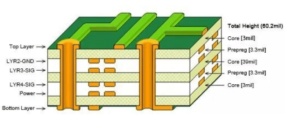
Stack-up Design Principles
A rational stack-up design is the foundation of impedance control. Multilayer boards are typically constructed by laminating core and prepreg layers alternately. Design should follow these principles:
- Symmetry: The stack-up structure should be symmetrical to prevent board warpage.
- Tight Coupling: Signal layers should be closely adjacent to their reference planes (small dielectric thickness).
- Solid Reference Planes: Each signal layer should have a solid reference plane (power or ground).
- Avoid Directly Adjacent Signal Layers: Prevent crosstalk between layers.
Differential Pair Design Principles
Differential signals transmit via a pair of opposite-phase signals, effectively suppressing common-mode noise. Differential impedance control requires attention to:
- Equal Length Routing: The length difference between the two differential traces should be minimized (typically < 50 mil).
- Constant Spacing: Maintain parallelism and consistent spacing between the two traces along their entire length.
- Tight Coupling: Trace spacing ≤ trace width to enhance noise immunity.
- Minimize Vias: Avoid unnecessary vias to prevent impedance discontinuities.
Impedance Calculation Tools
The most commonly used impedance calculation tool is Polar SI9000, which uses field solver algorithms to accurately calculate the characteristic impedance of various transmission line structures. The following parameters need to be input:
- Dielectric Constant (Er) of insulating material
- Trace Width (W1, W2, considering trapezoidal cross-section)
- Dielectric Thickness (H)
- Copper Thickness (T)
For example, select the “Coated Microstrip” model when calculating outer layer microstrip impedance to account for the solder mask effect. For preliminary design, simplified formulas can also be used for estimation: e.g., Microstrip Z₀ ≈ 87/√(εr+1.41) × ln[(5.98H)/(0.8W+T)].
Impedance Control Practices for Common Signals
High-Frequency Differential Signals (USB, HDMI)
USB differential pairs require 90Ω differential impedance, and HDMI requires 100Ω differential impedance. In a typical 4-layer board design, common parameters are: trace width 5 mil, spacing 7 mil, dielectric thickness 3.8-4.5 mil (based on FR-4 material). To reduce EMI risk, it is recommended to implement ground shielding for long-distance differential pairs, adding ground vias every 400 mil.
Memory Signals (DDR)
DDR memory signals typically require 50Ω single-ended impedance. For outer layer routing, a trace width of 5 mil with a distance of 3.8 mil to the reference plane yields approximately 55Ω impedance; increasing the trace width to 6 mil achieves an impedance closer to 50Ω. DDR routing requires providing a continuous return path; critical signals must not cross split planes.
Radio Frequency Signals (RF)
RF circuits typically require precise 50Ω impedance matching. Taking the RF module of the HackBat platform as an example, good impedance continuity is achieved by controlling trace width (0.133 mm) and dielectric thickness (0.1 mm), combined with a termination matching network (27 nH inductor and 0Ω resistor).
Summary
PCB impedance control is a core technology in high-speed circuit design, directly impacting system performance and stability. Successful impedance control requires collaborative optimization across the entire process, from stack-up design and material selection to routing strategies and manufacturing processes.
In the future, as signal rates continue to increase (e.g., PCIe 5.0/6.0, DDR5), requirements for impedance control will become even more stringent. Designers need a deeper understanding of material properties, adoption of more precise simulation tools, and close collaboration with PCB manufacturers to meet the growing severe high-speed design challenges.
Through the systematic introduction in this article, readers should grasp the basic principles and practical methods of impedance control, laying a solid foundation for high-speed circuit design. In actual projects, it is recommended to communicate impedance control requirements with PCB manufacturers early, utilize professional tools for simulation verification, and ensure the final product meets design expectations through TDR testing.


0 Comments