
Introduction
Within the intricate circuitry of high-performance electronic devices like smartphones and laptops, countless miniature chips are securely attached to printed circuit boards (PCBs) using sophisticated interconnection technologies. Among these, Ball Grid Array (BGA) assembly has emerged as a pivotal process for high-density, high-performance chip mounting, establishing itself as an indispensable core technology in modern electronics manufacturing. This article provides a comprehensive analysis of BGA‘s technical principles, its detailed process flow, and its critical role in advancing the electronics industry.

Fundamental Concepts of BGA Packaging
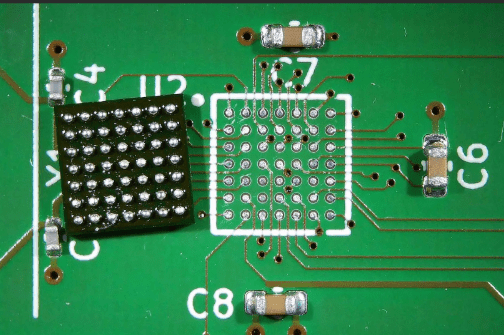
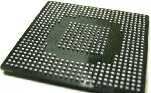
The Ball Grid Array (BGA) is an advanced integrated circuit (IC) packaging technology. Unlike traditional packages with leads protruding from their peripheries, BGA packages feature a grid of minute solder balls arranged in an array on the underside of the component. These solder balls serve the dual function of providing electrical interconnection pathways and ensuring mechanical attachment to the PCB. This innovative design enables a significantly higher number of input/output (I/O) connections within the same footprint, dramatically enhancing chip integration density, electrical performance, and thermal management.
Technical Advantages of BGA Packaging
BGA packaging offers substantial advantages over conventional packaging formats:
- High Interconnect Density: It efficiently meets the escalating demand for a large number of I/Os in complex modern chips, such as CPUs, GPUs, and FPGAs.
- Enhanced Electrical Performance: The shortened electrical pathways between the chip and the PCB reduce signal propagation delay, inductance, and electromagnetic interference (EMI), which is crucial for high-speed and high-frequency applications.
- Superior Thermal Dissipation: The direct thermal conduction path from the chip through the solder balls to the PCB significantly improves heat dissipation efficiency, supporting higher power operation.
- Improved Mechanical Reliability: The full-area array solder joint structure provides a robust mechanical connection, offering better resistance to shock and vibration compared to fine-leaded packages.
The BGA Assembly Process Flow
The BGA assembly process is a sequence of highly controlled and precise manufacturing stages. Each step is critical to ensuring the formation of reliable, defect-free solder connections.
Table: Key Stages in the BGA Assembly Process
| Process Stage | Description | Key Considerations |
|---|---|---|
| 1. Solder Paste Printing | A stencil is used to deposit precise amounts of solder paste onto the PCB’s bond pads. | Solder paste volume, alignment, and consistency are paramount to prevent bridging or insufficient solder. |
| 2. Component Placement | A high-precision pick-and-place machine accurately positions the BGA component onto the prepared PCB. | Placement accuracy is critical, as misalignment cannot be visually corrected after soldering. |
| 3. Reflow Soldering | The assembled board passes through a reflow oven with a precisely controlled thermal profile, melting the solder paste to form permanent solder joints. | The temperature profile (preheat, soak, reflow, cooling) must be meticulously optimized for the specific solder paste and component to prevent defects like tombstoning or voiding. |
| 4. Inspection & Testing | The hidden solder joints are inspected, primarily using Automated X-ray Inspection (AXI), followed by electrical tests. | AXI identifies hidden defects like bridging, voids, or misalignment. Electrical testing validates functional performance. |
The entire process demands a clean production environment, sophisticated equipment, and strict operational protocols to achieve the required high yield and reliability.
Key Technologies for Quality Inspection
Quality inspection for BGA assemblies presents a unique challenge due to the concealed nature of the solder joints beneath the component. Automated X-ray Inspection (AXI) has become an indispensable non-destructive quality control method, enabling the visualization and analysis of solder joints for defects such as bridging, cold solder joints, and voids. Additionally, electrical testing, in-circuit test (ICT), and boundary scan (JTAG) techniques collectively form a comprehensive quality assurance system to validate functionality and interconnection integrity.
Technical Challenges in BGA Assembly
Despite its significant benefits, BGA assembly involves several technical complexities:
- Rework Complexity: Repairing or replacing a faulty BGA component is a complex procedure that requires specialized hot-air rework stations, skilled technicians, and precise temperature control to avoid damaging the PCB or adjacent components.
- Thermal and Mechanical Stress Management: The difference in the coefficient of thermal expansion (CTE) between the silicon chip, the substrate, and the PCB can induce stress on solder joints during thermal cycling. For larger BGAs or harsh environments, an underfill process—dispensing an epoxy resin underneath the component—is often essential to redistribute stress and enhance long-term reliability.
- Higher PCB Demands: BGA technology imposes stricter requirements on PCB design and fabrication, including finer trace widths, higher layer counts, and more sophisticated via technologies (e.g., blind and buried vias), which increases overall cost and technical complexity.
Current Application Landscape Across Industries
BGA assembly technology is extensively utilized across various high-performance computing and electronics domains. It is the packaging method of choice for processors and graphics cards in consumer electronics, network chips in communication infrastructure, and core controllers in industrial automation, automotive electronics, and aerospace systems. BGA technology is fundamentally enabling the ongoing trend towards devices with smaller form factors, greater processing power, and enhanced functionality.
Future Development Trends
As semiconductor technology continues to advance, BGA packaging is also evolving. Its integration with cutting-edge approaches like 3D IC packaging and System-in-Package (SiP) is pushing the boundaries of integration density and system-level performance. Simultaneously, the adoption of new solder alloys, underfill materials, and substrate technologies is progressively addressing persistent challenges in thermal management, power integrity, and long-term reliability under demanding operating conditions.
Conclusion
As a vital pillar of modern electronics manufacturing, BGA assembly technology, with its unique high-density and high-performance attributes, has been a key driver behind the rapid miniaturization and performance growth of the entire electronics industry. While challenges in inspection, rework, and reliability management persist, continuous advancements in materials, processes, and design tools ensure that BGA technology will continue to play a critical role in future electronic product innovation. A deep understanding and mastery of this technology remain of significant value for engineers and technicians engaged in electronics design, manufacturing, and related fields.


0 Comments