
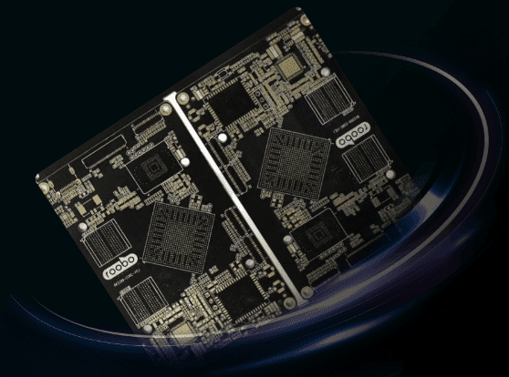
What is an HDI PCB? – The Backbone of Modern Electronic Devices
HDI PCBs (High-Density Interconnect Printed Circuit Boards) are among the most critical fundamental components in today’s electronics industry, representing the forefront of printed circuit board technology development. HDI refers to circuit board design and manufacturing technology that utilizes micro-blind and buried via technology to achieve high-density circuit distribution. Compared to traditional PCBs, HDI boards provide more interconnection points per unit area, enabling electronic devices to implement more complex functions within a smaller space. As the “Mother of Electronic Products,” the quality of a PCB directly impacts the performance and reliability of the entire electronic system, and HDI technology elevates this fundamental component to new heights.
Since its inception, HDI technology has rapidly proliferated alongside the trend towards thinner, lighter, and more multifunctional electronic products. From the first 32-bit computer introduced by Hewlett-Packard in 1985 to today’s high-end servers utilizing 36 sequential lamination multilayer boards and stacked microvias, HDI/microvia technology is undoubtedly the future of PCB architecture. Modern large-scale ASICs and FPGAs, with their smaller device pitches, more I/O pins, and embedded passive components, demand smaller PCB feature sizes, driving strong demand for HDI/microvias.
The Technical Core of HDI PCBs – The Microvia Revolution
The most significant technical characteristic of HDI PCBs lies in the adoption of microvia technology, replacing traditional through-hole technology. Traditional PCBs primarily use through-holes formed by mechanical drilling, which penetrate all board layers and occupy significant space. In contrast, HDI boards utilize laser drilling to create microvias with diameters less than 150 micrometers. These microvias can connect only specific layers, thereby greatly enhancing routing density.
Via Type Comparison Table
| Via Type | Connection Method | Manufacturing Method | Diameter Range | Application Characteristics |
|---|---|---|---|---|
| Through-hole | Connects all layers | Mechanical Drilling | > 0.2mm | Low cost, high reliability, large space consumption |
| Blind Via | Connects outer layer to inner layer(s) | Laser Drilling | < 0.15mm | Saves space, increases outer layer routing density |
| Buried Via | Connects inner layer to inner layer | Laser Drilling | < 0.15mm | Does not occupy outer layer space, increases inner layer interconnects |
| Stacked Via | Multiple blind/buried vias stacked vertically | Laser Drilling + Filling & Plating | < 0.15mm | Highest interconnect density, complex process |
The core advantage of microvia technology is the significant improvement in space utilization. Standard multilayer boards use through-holes to connect different layers, but these through-holes occupy substantial space that could otherwise be used for routing. Conversely, using blind/buried vias to achieve interlayer connections frees up space for more routing lines, thereby increasing routing density. Simultaneously, laser drilling enables smaller hole diameters compared to mechanical drilling, further conserving space.
The Manufacturing Process of HDI PCBs – The Art of Precision
The manufacturing process for HDI PCBs is complex and precise, involving multiple critical process steps with technical requirements far exceeding those of traditional PCBs. The process begins with the raw material preparation stage. HDI boards typically use special materials, such as high Tg (Glass Transition Temperature) laminates, Resin Coated Copper (RCC) foil, etc., which offer better dimensional stability and resistance to conductive anode filament (CAF) formation.
Next is the lamination and imaging stage, which forms the foundation of the multilayer structure. HDI boards are manufactured using the build-up method, progressively constructing complex multilayer structures through multiple cycles of pressing, imaging, and etching. The number of build-up layers directly correlates with the board’s technical grade – standard HDI boards typically involve 1 build-up cycle, while high-end HDI employs 2 or more build-up cycles.
Laser drilling is a core step in HDI manufacturing. Unlike traditional mechanical drilling, laser drilling uses high-energy laser beams (e.g., CO2 or UV lasers) to ablate the resin dielectric layer, forming tiny blind or buried vias. Laser systems primarily operate via two mechanisms: photothermal ablation, which heats the material causing melting and evaporation, and photochemical ablation, which uses high-energy photons to directly break chemical bonds in the material. After laser drilling, hole metallization is required, using electroless copper deposition or direct plating techniques to form a conductive layer on the hole walls, establishing electrical connections between different layers.
As the HDI tier increases, manufacturing process complexity grows exponentially. A 2-tier HDI board requires two outer copper foil lamination cycles, two drilling processes, and two laser drilling processes. Taking an 8-layer board with blind/buried vias as an example, layers 2-7 are first laminated together, and the buried vias connecting layers 2-7 are fabricated. Then, layers 1 and 8 are added via lamination, and through-holes penetrating layers 1-8 are drilled to complete the board. This complex process flow demands extremely high registration accuracy and process control; even a minor deviation in any step can render the entire board defective.
HDI PCB Design Principles – Balancing Performance and Manufacturability
Successful HDI design requires finding the optimal balance between performance, cost, and manufacturability. First, stack-up planning is fundamental, requiring rational allocation of layer functions based on signal integrity, power integrity, and thermal management needs. For high-speed digital circuits, a design with adjacent ground and power planes is commonly used to provide clear return paths and controlled impedance.
Impedance control is a key consideration in high-speed circuit HDI design. Designers need to precisely calculate signal trace width, spacing, and dielectric thickness to achieve target impedance values (typically 50Ω single-ended or 100Ω differential). This requires designers to have a deep understanding of the laminate’s Dielectric Constant (Dk) and Dissipation Factor (Df), and how these properties vary with frequency.
Microvia layout strategy directly impacts the routing density and signal quality of the HDI board. Designs can primarily employ two approaches: staggered vias or stacked vias. Staggered via design is relatively simpler and lower cost but consumes more space. Stacked via design maximizes space utilization but places extremely high demands on the plating and via filling process, significantly increasing cost.
Signal integrity analysis is an indispensable part of modern HDI design. This includes timing analysis, crosstalk control, and power distribution network design, among others. For RF/microwave applications, Electromagnetic Compatibility (EMC) and Radio Frequency Interference (RFI) must also be considered. Modern EDA tools (e.g., Cadence Allegro, Mentor PADS) provide a suite of simulation functions to help designers predict and optimize circuit performance before physical manufacturing.
Application Areas of HDI PCBs – From Consumer Electronics to High-End Technology
HDI PCBs were initially used mainly in high-tech fields like aerospace and military, but with technology proliferation and cost reduction, they have rapidly expanded into nearly all electronic sectors. The following are the primary application scenarios for HDI technology:
Consumer Electronics
Smartphones represent the largest application market for HDI boards, with over 90% of smartphone motherboards utilizing HDI technology. Modern smartphones typically use 8-layer 1-tier to 10-layer 2-tier HDI boards, while high-end models like the iPhone feature motherboards with complexities reaching 5-tier HDI. Furthermore, compact consumer electronics like tablets, digital cameras, and wearable devices also widely use HDI technology to meet their dual demands for miniaturization and high performance.
Automotive Electronics
With the acceleration of vehicle electrification and智能化, the demand for HDI boards in automotive electronic systems is growing rapidly. HDI technology is widely used in Advanced Driver-Assistance Systems (ADAS), in-vehicle infotainment systems, and Battery Management Systems (BMS). Notably, lidar systems used in autonomous driving, which require high resolution, strong anti-interference capability, and small size, primarily use HDI boards.
High-Speed Communication and Computing
High-end applications like AI servers and data center equipment are becoming new growth drivers for HDI technology. Key components within AI servers, such as GPU motherboards, OAM accelerator cards, and network interface cards, are increasingly adopting high-tier HDI solutions. For instance, NVIDIA’s GB200 NVL72 system employs complex HDI design to support high-speed interconnect bandwidths up to 900 GB/s.
HDI Board Tiers and Classification – From Simple to Complex
Based on complexity, HDI boards can be classified into various types such as 1-tier, 2-tier, 3-tier, 4-tier, and Any-layer HDI. This classification reflects the level of precision and manufacturing difficulty.
Comparison of Characteristics of Different HDI Tiers
| HDI Tier | Structure Notation | Technical Characteristics | Typical Applications |
|---|---|---|---|
| 1-tier HDI | 1+N+1 | One build-up cycle, laser vias on two outer layers | Feature phones, basic digital products |
| 2-tier HDI | 2+N+2 | Two build-up cycles, two layers of laser vias are staggered | Smartphones, Tablets |
| 3-tier HDI | 3+N+3 | Three build-up cycles, higher interconnect density | High-end smartphones, thin-and-light laptops |
| Any-layer HDI | Any-layer interconnect | Direct connection possible between any layer, highest density | Flagship phones, military equipment |
1-tier HDI boards have the simplest structure, requiring only one outer copper foil lamination cycle, involving one initial core lamination, one drilling process, one outer copper foil lamination, and one laser drilling process. As the tier increases, manufacturing complexity rises sharply. 2-tier HDI requires two outer copper foil lamination cycles (i.e., processes involving two outer copper foil laminations, two drilling steps, and two laser drilling steps). Using the earlier 8-layer blind/buried via board example, layers 2-7 are first laminated and their buried vias fabricated, before adding layers 1 and 8.
Any-layer HDI represents the current peak of technology, allowing direct interconnection between any two layers and offering maximum design flexibility. Manufacturing this structure requires layered laser drilling followed by sequential lamination, resulting in the most complex circuit density and process difficulty. Furthermore, Substrate-like PCBs (SLP), which represent a further development based on HDI technology, utilize the modified Semi-Additive Process (mSAP) to achieve finer line width and spacing, constituting the current highest-end HDI technology.
Market Prospects and Challenges for HDI PCBs – Coexisting Opportunities and Competition
The HDI PCB market is experiencing rapid growth, primarily driven by trends such as the proliferation of 5G communication, the explosion of AI technology, and automotive electronics. According to Prismark data, the global PCB market size for servers and related system components was approximately $5.177 billion in 2023, and is projected to grow at a 9% CAGR to reach $7.974 billion by 2028. HDI boards, being the fastest-growing category within this segment, are expected to achieve a Compound Annual Growth Rate (CAGR) of 16.3% from 2023 to 2028.
Regarding market structure, HDI production capacity was initially concentrated in Europe, America, Japan, and South Korea. However, due to cost pressures and industry transfer, China has become the world’s largest HDI producer. Nevertheless, the technological barriers for high-tier HDI boards, especially Any-layer HDI and SLPs, remain high and are still dominated by a few leading companies. As emerging applications like AI servers increase demand for high-tier HDI, the technology landscape may face restructuring, presenting an opportunity for Chinese manufacturers with strong technical capabilities to overtake competitors.
The main challenge facing HDI manufacturing lies in process complexity and yield control. Because HDI employs the build-up manufacturing method, each additional tier requires extra processes like lamination, drilling, and plating, which reduces production capacity. More critically, the yield of each process step must be extremely high for the overall high-tier HDI board to maintain an acceptable final yield. For example, if the composite yield per process stage is 90%, the overall yield for a 2-tier HDI board drops to 81%, and further to 72.9% for a 3-tier board. This cumulative yield effect makes high-tier HDI manufacturing highly challenging.
Summary
HDI PCB technology, as the cornerstone of modern electronics manufacturing, has enabled leaps in the miniaturization and performance enhancement of electronic devices through microvia technology. From smartphones to AI servers, from medical equipment to smart vehicles, HDI technology underpins today’s most cutting-edge electronic innovations, embodying the trend towards higher density and performance in electronic products.
With the continuous advancement of technologies like 5G, IoT, AI, and automotive electronics, HDI technology faces new opportunities and challenges. Future HDI development will trend towards higher tiers, finer line width/spacing, and deeper integration with advanced technologies like System-in-Package (SiP). Simultaneously, sustainable development and environmentally friendly materials will also become important directions for HDI technology evolution.
For electronics engineers and designers, mastering HDI technology not only means keeping pace with technological development but is also a key capability for developing the next generation of innovative products. As electronic devices continue evolving towards higher performance and smaller size, the pace of HDI technology innovation will not cease. It will continue to serve as a core driving force for progress in the electronics industry, connecting every corner of the physical and digital worlds.


0 Comments