
Introduction: The Importance of Power Supply PCB
The Power Supply PCB (Printed Circuit Board) serves as the heart of modern electronic equipment. It is specifically designed to carry and interconnect electronic components related to power management, undertaking the critical task of efficiently and stably converting input power into the required DC voltage for the device. Unlike standard signal PCBs, Power Supply PCBs must handle larger currents, higher voltage variations, and effectively manage the resulting heat and electromagnetic interference. Their design quality directly impacts the stability, efficiency, and safety of the entire electronic system.
Amid the trend towards miniaturization and higher efficiency in modern electronics, Power Supply PCB design has evolved into a comprehensive discipline integrating electrical engineering, thermodynamics, and Electromagnetic Compatibility (EMC). Whether for simple linear regulators or complex switching power supply systems, excellent PCB layout and routing are fundamental to ensuring power supply performance meets design targets.
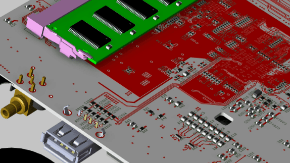
Basic Structure and Composition of Power Supply PCB
Power Supply PCBs possess distinct structural characteristics to accommodate high-current transmission and heat dissipation requirements:
- Conductive Layer: Typically utilizes thicker copper foil (1oz to 4oz or even thicker) as current pathways to reduce impedance and losses.
- Dielectric Layer: Uses insulating materials like FR-4 as the substrate, providing mechanical support and electrical insulation.
- Protective Layer: Includes the solder mask (prevents short circuits and oxidation) and silkscreen layer (marks component information).
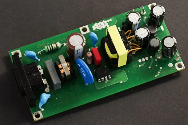
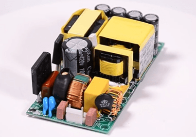
The core functional sections of a Power Supply PCB typically include input filtering circuits, power switching or regulation circuits, control circuits, output rectification/filtering circuits, and feedback networks. These sections require rational partitioning and placement based on current magnitude, voltage level, and noise sensitivity to ensure stable and reliable power supply operation.
Core Elements of Power Supply PCB Design
Board Layer and Copper Thickness Selection
Depending on the power supply’s complexity and performance requirements, Power Supply PCBs can be designed as single-layer, double-layer, or multi-layer boards. Simple linear power supplies might only require 1-2 layers, whereas complex switching power supplies often need 4 or more layers to provide complete ground and power planes. Multi-layer board structures facilitate better impedance control, provide low-noise reference planes, and improve Electromagnetic Compatibility.
Copper thickness selection directly relates to current-carrying capacity. Standard PCBs generally use 1oz (35μm) copper thickness, capable of carrying approximately 1.5A current (for 1mm trace width). For high-current power supplies, increased copper thickness (2oz or above) or wider trace widths are necessary to ensure sufficient current capacity and heat dissipation performance.
Safety Standards and Creepage/Clearance Distances
Power Supply PCB design must comply with safety regulation, especially for sections involving high voltage. Key safety distances include:
- Clearance: The shortest distance measured through air. For example, with an input voltage of 50V-250V, the spacing between L-N lines before the fuse should be ≥1.7mm.
- Creepage Distance: The shortest distance measured along the surface of the insulation. Under the same conditions, this should be ≥2.5mm.
- Primary and Secondary Sides: An isolation distance of ≥6.4mm should be guaranteed. Slotting under components like optocouplers can be used when necessary to enhance insulation.
These safety requirements are fundamental to ensuring the safety and reliability of power supply products and must strictly adhere to international and industry standards.
Layout Planning and Optimization Strategies
Component Placement Principles
The layout quality of a Power Supply PCB has a decisive impact on performance. A rational layout should adhere to the following principles:
- Compact Layout: The power loop (switching loop) should be as compact as possible to minimize loop area, thereby reducing electromagnetic radiation and parasitic inductance.
- Priority Placement of Key Components: Place core components like transformers, power switches, and filter capacitors first, followed by the control circuitry.
- Input/Output Isolation: Clearly demarcate input and output areas to avoid cross-contamination. Noise sources should be kept away from input/output terminals.
Thermal Design Considerations: Heat-generating components (power transistors, rectifiers) should be evenly distributed and located near heat sinks or board edges to facilitate heat dissipation.
Power Loop Design
Switching power supplies contain four key current loops, each with different characteristic requirements:
- Power Switch AC Loop: Contains high-amplitude trapezoidal current with high harmonic content; should be minimized as much as possible.
- Output Rectifier AC Loop: Also contains high di/dt current; requires minimized loop area.
- Input Source Current Loop: Approximates DC current; has relatively lower routing requirements.
- Output Load Current Loop: DC output; still requires a low-impedance path.
The layout sequence for these loops should be: route the switching and rectifier loops first, then the control circuit, and finally the input and output loops. The three main components of each loop (filter capacitor, switch/rectifier, inductor/transformer) should be placed adjacent to each other, keeping the current path as short as possible.
Routing Techniques and Current Handling
Trace Width vs. Current Relationship
Power trace widths must be carefully designed based on current magnitude to avoid overheating and excessive voltage drop. Empirical data indicates that for a copper thickness of 50μm (approx. 1.4oz), a 1mm wide trace can safely carry 1A current (with temperature rise not exceeding 3°C). For 2oz (70μm) copper thickness, the same width can carry approximately 1.5A. High-current paths should use widened traces or copper pours to increase the conductive cross-section.
Via Design
Vias are used for inter-layer connections; their number and size must meet current requirements. Experiments show that a single 10mil (0.25mm) via can safely pass approximately 1-1.5A current. High-current paths should employ multiple vias in parallel, using filled and plated via processes to enhance current-carrying capacity and heat dissipation.
Special Signal Handling
- Feedback Paths: Voltage feedback traces should be routed away from noise sources, use a 20mil width, and avoid interference.
- Drive Signals: MOSFET gate drive lines should be short and thick (≥15mil) to reduce inductive effects and ensure fast switching.
- Sampling Signals: Weak signals like current sensing require differential pair routing and should be kept away from interference sources.
Thermal Management and Heat Dissipation Design
Energy loss during power conversion is transformed into heat. Effective thermal management is crucial for ensuring reliable operation and long-term reliability of the power supply.
Heat Dissipation Pathways
- Copper Foil Dissipation: Utilize the power layer copper foil itself as a dissipation path by widening traces or using copper pours to increase surface area.
- Thermal Vias: Place arrays of thermal vias underneath heat-generating components to conduct heat to the other side or internal layers of the PCB.
- External Heat Sinks: Attach heat sinks to high-power devices, optimizing thermal contact using thermal interface materials.
Layout Optimization
Temperature-sensitive critical components (e.g., ICs) should be placed away from heat-generating elements. Components sensitive to temperature, such as electrolytic capacitors, also need distance from heat sources to prevent shortened lifespan due to high temperatures. Heat-generating components should be evenly distributed to avoid forming local hot spots, while also considering airflow design to ensure good ventilation.
EMC and Signal Integrity
Electromagnetic Compatibility Design
The fast switching actions in switching power supplies are strong sources of electromagnetic interference, making good EMC design essential:
- Minimize Loop Area: The smaller the high-frequency loop area, the weaker the electromagnetic radiation. Minimize the area of switching and rectifier loops.
- Single-Point Grounding: Connect power ground and signal ground at a single point to avoid common-mode interference caused by ground loops.
- Shielding and Isolation: Employ local shielding for particularly sensitive circuits or strong noise sources. Create isolation slots between primary and secondary sides of transformers if necessary.
Power Integrity
Power Integrity (PI) measures the quality of power delivery to the load. Key measures include:
- Decoupling Capacitors: Place decoupling capacitors of appropriate value near IC power pins to provide local charge storage and reduce power supply impedance.
- Bypass Capacitors: Used to filter high-frequency noise; should be placed close to device power pins.
- Power Plane Design: Use solid power and ground planes in multi-layer boards to provide a low-impedance power distribution path.
Summary and Future Development Trends
Power Supply PCB design is a complex systems engineering task requiring comprehensive consideration of electrical performance, thermal management, safety standards, and EMC, among other factors. Excellent Power Supply PCB design should follow the principles of “Power First, Signal Second” (layout power loops before control loops) and “Strong Currents First, Weak Signals Second” (layout power sections before signal sections), ensuring power paths are short and wide, and control signals are distant from noise sources.
Future Power Supply PCB design will face the following development trends:
- High-Density Interconnect (HDI): As devices miniaturize, achieving higher power density within limited space becomes a key challenge.
- Higher Frequency Operation: Increasing switching frequencies helps reduce passive component size but imposes higher demands on PCB materials and high-frequency layout.
- Integration: Integrating more functions (e.g., driving, protection) into power modules simplifies peripheral circuits.
- Thermal Management Innovation: New thermal conductive materials and cooling technologies will address the heat dissipation needs of higher power densities.
- Intelligent Design Tools: Utilizing simulation-driven design to predict and resolve potential power integrity and thermal issues proactively.
With the rapid development of emerging technologies like 5G, IoT, and new energy vehicles, the importance of Power Supply PCB design will become even more prominent. Engineers need to continuously update their knowledge base and master new materials, processes, and design methodologies to meet increasingly stringent power design challenges.


0 Comments