
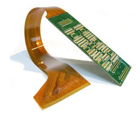
Flexible PCB (FPC) are a rapidly developing electronic interconnect technology that is increasingly becoming an important choice in electronic design due to their excellent flexibility and high reliability. They are also known as flexible electronics, flexible circuits, or flexible printed circuits.
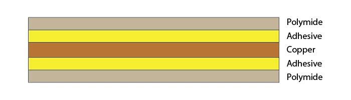
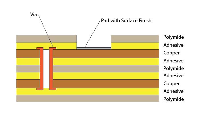
The conductive lines of a flexible PCB are built on a flexible plastic substrate, commonly made of materials such as polyimide (PI), PEEK, and polyester (PET). Components are fixed to exposed copper pads by soldering.
Depending on design requirements, flexible PCB can be single-layer, double-layer, or multi-layer structures. Because of the flexibility of their substrate, they can be freely bent, folded, or rolled within a limited space, offering greater packaging flexibility compared to rigid PCB. Flexible PCB can not only accommodate the same electronic components as rigid PCB but also seamlessly integrate with traditional manufacturing processes, providing thinner, lighter, and more efficient interconnect solutions for modern electronic products.
Flexible PCB VS Traditional PCB?
Traditional PCB (rigid circuit boards) typically use fiberglass cloth as the substrate, possessing high strength and rigidity, providing stable support for components and good heat dissipation. These circuit boards are widely used in electronic devices where structural stability is critical.
In contrast, flexible PCB use flexible substrates such as polyimide (PI), allowing the board to be bent, folded, and adapt to complex spatial structures. Their excellent vibration resistance, heat dissipation, and lightweight properties make them ideal for compact electronic products such as smart wearable devices, mobile phones, and cameras.
Besides the differences in substrate and structure, flexible PCB differ from traditional PCB in the following significant ways:
Conductive Material: To accommodate bending requirements, flexible PCB typically use rolled annealed copper (RA copper) instead of traditional electrolytic copper.
Manufacturing Process: Flexible PCB use a coverlay instead of solder mask to protect exposed circuitry and maintain flexibility.
How to maximize space utilization in flexible PCB?
Flexible PCB, with their bendable, ultra-thin, and easily moldable characteristics, can flexibly conform to the complex internal structures of devices, achieving efficient space utilization. Compared to traditional rigid circuit boards, flexible PCB can be folded, rolled, or bent for mounting, making the internal layout of electronic systems more compact and providing strong support for device miniaturization and weight reduction.
In rigid-flexible circuit design, flexible PCB not only connect different functional modules in limited space but also allow devices to be mounted in a multi-directional distribution, saving assembly space while ensuring the reliability and stability of signal transmission.
Furthermore, the combination of flexible PCB and High-Density Interconnect (HDI) technology enables circuits to achieve higher integration in a smaller area. HDI designs support finer lines, smaller vias, and thinner laminated structures, resulting in compact, high-performance circuit systems.
With these advantages, flexible PCB have become an ideal choice for meeting the requirements of high-density wiring, precision structures, and compact packaging. In space-constrained devices, they are often key to achieving high-performance connectivity and lightweight design. For components that require rigid support (such as chips or high-precision sensors), designers can also mount them on the HDI layer and then achieve reliable interconnection with other modules through flexible circuits, thus achieving a perfect balance between “rigidity and flexibility”.
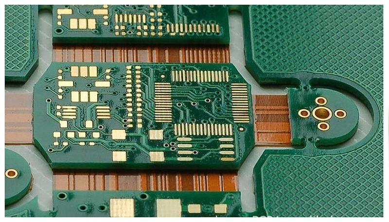
How can multilayer FPC be bonded more stably?
In multilayer FPC or rigid-flex PCB, the choice of adhesive is crucial to structural stability. Inappropriate adhesives can lead to delamination, reduced flexibility, or failure under thermal stress. To ensure more stable adhesion, materials must be selected appropriately based on the application environment.
- Common adhesive types include:
Acrylic adhesives: Possessing excellent flexibility and adhesion, they can withstand temperatures up to 150°C and have good moisture and chemical resistance, making them suitable for most flexible applications.
Epoxy adhesives: Known for their high strength and heat resistance (up to 180°C), they are suitable for high-temperature environments, but have lower flexibility and are not suitable for designs requiring frequent bending.
Adhesive-free lamination: Polyimide is directly bonded to a rigid layer via hot pressing, reducing thickness and improving thermal stability, but the manufacturing process is more complex.
- When selecting an adhesive solution, the following factors should be considered:
Thermal resistance: Ensure the adhesive can withstand the operating temperature of the equipment; epoxy or adhesive-free solutions are recommended for high-temperature applications.
Flexibility: For designs requiring frequent bending, acrylic adhesives should be preferred.
Thickness control: Thin-layer (12-25μm) adhesives reduce stack-up thickness, suitable for compact designs.
Dielectric properties: Adhesives with low dielectric constants (approximately 3.0-3.5) help reduce high-frequency signal interference.
By comprehensively considering thermal, flexibility, and electrical properties, designers can achieve a balance between performance and stability, resulting in stronger and more reliable bonding of multilayer flexible PCB.
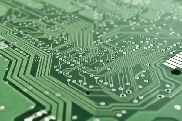
What is the etching process?
Etching is a crucial step in FPC manufacturing, used to remove excess copper layers and form the desired circuit pattern.
At approximately 45±5°C, etching solution is evenly sprayed onto the copper foil surface through a nozzle. This solution reacts with areas not protected by etching resists via an oxidation-reduction reaction, removing excess copper. Following a stripping process, the desired circuit structure is exposed, completing the circuit formation.
The main components of the etching solution include: copper chloride, hydrogen peroxide, hydrochloric acid, and soft water (concentration must be strictly controlled).
Key quality control points: The dry film must be firmly adhered; there should be no erosion, peeling, or breakage at solder joints.
Control the etching speed to avoid over-etching that leads to thinner lines; line width and total pitch should be key monitoring parameters.
Ensure even spraying of the etching solution to prevent uneven etching on both sides or different areas of the same side.
There must be no residual copper on the board surface, especially for double-sided FPC.
No residual adhesive should be present to avoid exposed copper or poor plating adhesion.
After stripping, the FPC board should be free of oil stains, impurities, or defects such as peeling copper foil.
During storage and handling, prevent the board from being jammed or oxidized.
By precisely controlling the etching temperature, chemical solution ratio, and spray uniformity, clear circuit patterns and dimensional stability can be ensured, thereby improving the overall quality and reliability of the flexible PCB.
How to control the accuracy of layering and drilling?
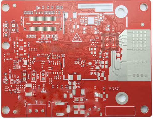
In high-speed PCB design, layer stack-up and drilling precision directly impact signal integrity and overall performance. With data rates exceeding 10Gbps, even minute manufacturing errors can lead to signal attenuation, crosstalk, or electromagnetic interference (EMI).
Controlled-depth drilling is a critical process used to remove unused portions of vias in plated through-hole (PTH) circuits, known as “stubs.” These stubs, if retained, act like antennas, causing signal reflections and impedance mismatches, affecting high-speed signal transmission. By precisely controlling the drilling depth, manufacturers can effectively eliminate stubs, ensuring cleaner signal paths and lower latency, thereby improving the high-speed stability of the circuit.
However, achieving high-precision layer stack-up and drilling control still presents the following challenges:
Manufacturing Precision: Deviations in drilling depth exceeding 0.05 mm can damage active layers or leave residual copper and vias.
Design Complexity: Back-drilling designs with numerous vias in multilayer boards increase layout and documentation complexity, requiring close collaboration with the manufacturer.
Despite the challenges of cost and manufacturing processes, precise control of stack-up and drilling accuracy remains an indispensable key element for ensuring stable performance in applications with extremely high signal quality requirements, such as high-speed communication and server systems.
How can FPC surface treatment be made more reliable?
Surface treatment adds a protective layer to the copper layer of a PCB, effectively preventing copper oxidation or rust and ensuring long-term stable circuit operation. It also improves solderability, making it easier to securely connect electronic components during assembly. Without surface treatment, the copper layer will quickly oxidize or wear down, ultimately leading to poor electrical connections or even PCB failure.
| Purpose/Function | Introduction |
| Prevent oxidation | Stop the copper to prevent rust and keep the PCB working properly. |
| Prevent corrosion | Prevent rust and damage, and ensure a secure connection. |
| Create a weldable surface | This makes it easier and safer to connect parts during the assembly process. |
Surface treatment effectively protects the copper layers on a PCB, preventing oxidation, rust, or damage caused by air or moisture. Without this protection, the copper will gradually deteriorate, making the PCB more prone to breakage or failure.
- Common surface treatment methods include:
OSP: Forms an ultra-thin protective film, isolating it from air and preventing copper oxidation;
HASL: Provides a robust solder coating, enhancing durability;
ENIG, ENEPIG: High-end processes offering better protection and a longer lifespan.
Choosing the appropriate surface treatment can significantly improve the reliability and lifespan of a PCB, ensuring stable operation in various environments.
FPC curing and cutting molding
In the manufacturing process of flexible printed circuit boards (FPC), curing and cutting are crucial steps to ensure product performance and appearance quality.
The cover film of FPC is typically composed of a polyimide (PI) film and a semi-cured epoxy resin adhesive, with a release liner applied to the surface to prevent contamination. This multi-layered structure provides excellent insulation and adhesion during subsequent thermosetting and curing, offering stable protection for the circuitry.
In the forming stage, laser cutting technology is gradually replacing traditional die-cutting processes. Laser cutting offers advantages such as high precision, non-contact operation, and no mechanical stress. It effectively avoids stretching or indentation caused by mold extrusion and enables micron-level precision machining, making it particularly suitable for manufacturing high-density circuitry and micro-via structures.
This process not only reduces mold costs and improves yield rates but also significantly enhances production efficiency and product consistency, making it the ideal solution for opening windows and forming FPC cover films.
Assembly and System Integration
In the design of miniaturized electronic devices, engineers must strike a balance between limited space and high-performance requirements. Achieving high-speed communication demands not only precise signal integrity but also stable system operation under vibration, shock, and extreme temperature conditions. Furthermore, interconnect structures must be optimized for compact spaces to improve assembly efficiency and reduce design complexity.
FPC, with their thinness, flexibility, and high reliability, are an ideal solution. They can integrate shielding layers and impedance control structures, effectively reducing signal loss and increasing data transmission rates; enhanced thermal management ensures stable reliability even at high temperatures. Smaller bending radii allow FPC to flexibly adapt to complex structures, making them particularly suitable for space-constrained devices or those subjected to frequent mechanical stress.
Thindry FPC, for example, excel in signal integrity, ease of assembly, and environmental adaptability. Precise impedance control and shielding design ensure stable high-speed data transmission; simultaneously, their thermal resistance up to +130°C meets the demands of demanding industrial and consumer electronics applications, enabling devices to achieve higher performance and more reliable system integration.
Advantages of Flexible PCB in Modern Applications
A deep understanding of the manufacturing process of flexible printed circuit boards (PCB) clearly reveals their importance in modern electronic design. Flexible PCB not only provide products with higher integration and reliability but also greatly expand the possibilities of engineering design. Their main advantages include:
Space and weight savings: Flexible PCB can replace traditional connectors and cables, reducing overall size and weight by up to 60%, making them particularly suitable for lightweight and compact designs.
Excellent durability: Thanks to the high ductility of the flexible substrate, some designs can withstand more than 200,000 bending cycles while maintaining excellent performance.
Greater design freedom: Flexible circuits can adapt to complex three-dimensional structures, enabling more creative design solutions for wearable devices, medical instruments, and aerospace products.
Higher system reliability: Fewer connection points mean fewer potential sources of failure, significantly improving the overall system stability and lifespan.
Flexible PCB, with their lightweight, high reliability, and design flexibility, are becoming an indispensable core technology in modern electronic systems. From smart wearables to high-end industrial equipment, they meet the demands for miniaturization, high speed, and high reliability with their superior performance. With continuous advancements in manufacturing processes and materials technology, flexible PCB will continue to drive innovation and development in electronic products.


0 Comments