
Introduction
In today’s highly integrated electronic devices, the performance of Integrated Circuits (ICs) continues to improve while their physical size keeps shrinking. This development trend poses unprecedented challenges for chip packaging technology. As a key intermediary connecting the chip and the Printed Circuit Board (PCB), the IC Substrate (or Interposer) has emerged and gradually become an indispensable core component in advanced chip packaging. The IC substrate not only provides physical support and protection for the chip but also serves as a critical carrier for achieving high-density electrical interconnection, signal transmission, power distribution, and thermal management.
As semiconductor process nodes continuously approach physical limits, relying solely on shrinking chip size to enhance performance has become increasingly difficult. In this context, advanced packaging technologies, particularly 2.5D/3D packaging solutions based on IC substrates, are becoming an important path to extend Moore’s Law. According to statistics, the global IC substrate market size exceeded $12 billion in 2023 and is expected to reach $21 billion by 2028, with a Compound Annual Growth Rate (CAGR) of approximately 11.8%. This data fully reflects the important position of IC substrates in the modern electronics industry and indicates their broad development prospects for the future.
1. What is an IC Substrate?
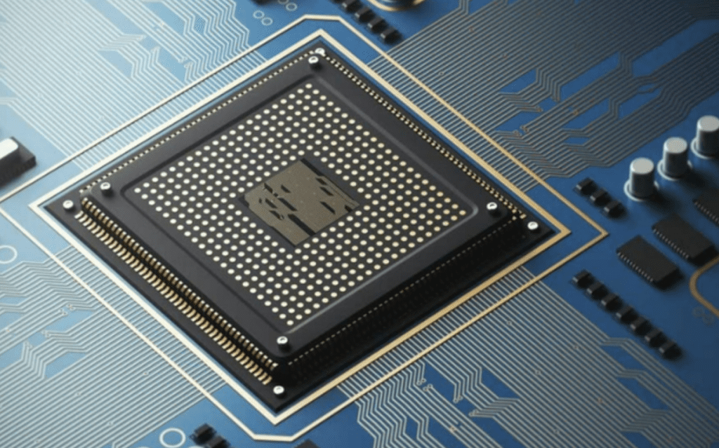
An IC substrate, also known as an interposer or silicon interposer, is a high-density interconnect substrate that provides electrical connection and mechanical support between the chip and the conventional PCB. Structurally, an IC substrate is essentially a printed circuit board with ultra-high wiring density, but its technical parameters far exceed those of ordinary PCBs. The core function of an IC substrate is to address the “interconnect gap” between the chip and the motherboard – that is, the mismatch between the very fine pin pitch on the chip side (which can be as small as 20μm) and the relatively larger pad pitch on the PCB side (typically 100-200μm).
Classified by material, IC substrates are mainly divided into three categories: organic substrates, ceramic substrates, and silicon substrates. Organic substrates typically use BT resin (Bismaleimide Triazine) or ABF (Ajinomoto Build-up Film) as the dielectric material, combined with copper traces. Their characteristic is relatively low cost, making them suitable for most consumer electronic chips. Ceramic substrates use alumina (Al₂O₃) or aluminum nitride (AlN) as the base material, offering excellent thermal stability and high-frequency characteristics, primarily used in aerospace and military fields with high reliability requirements. Silicon substrates use silicon as the base material and utilize mature semiconductor processes to create fine traces, enabling the highest interconnect density, often used in high-end applications like 2.5D/3D integration.
In terms of technical parameters, IC substrates differ significantly from conventional PCBs. Taking line width and spacing as an example, the line width/space of a standard PCB is typically above 50μm/50μm, whereas high-end IC substrates can achieve line width/space of 2μm/2μm, an improvement of over 25 times. Regarding via diameter, the microvia diameter of an IC substrate can be as small as 10μm, while the mechanical drilling limit for ordinary PCBs is about 100μm. Furthermore, the number of routing layers in an IC substrate is typically 1-10 layers. Although this is fewer than high-end PCBs (which can have over 30 layers), the interconnect density per unit area is several orders of magnitude higher.
2. Characteristics and Features of IC Substrates
As a critical component of advanced packaging, IC substrates possess a series of unique performances and characteristics that make them play an irreplaceable role in complex electronic systems.
High-Density Interconnect Capability is the most notable feature of IC substrates. With the dramatic increase in the number of chip I/Os (the pin count of high-end GPUs has exceeded 10,000), traditional packaging technologies can no longer meet such high-density interconnection demands. IC substrates, through fine-line processing technology, can achieve wiring densities with line width/space as low as 2μm/2μm, sufficient to handle the most complex chip interconnection requirements. For example, in TSMC’s CoWoS (Chip-on-Wafer-on-Substrate) packaging, the copper micro-bump pitch on the silicon interposer can be as small as 40μm, allowing multiple chips to achieve high-speed, high-bandwidth interconnection through the substrate.
Excellent Thermal Management Performance is another important characteristic of IC substrates. Modern high-performance chips have extremely high power density. For instance, the power of CPUs and GPUs can exceed 300W, and the continuous reduction in chip size leads to heat flux density exceeding 100W/cm². Silicon substrates, due to the use of silicon material, have a thermal conductivity (about 150 W/m·K) much higher than that of organic substrates (about 0.2-0.3 W/m·K), enabling effective conduction of heat generated by the chip. For applications with particularly high power, aluminum nitride ceramic substrates (with thermal conductivity reaching 170-200 W/m·K) become the preferred choice, widely used in microwave radio frequency and power electronics fields.
Good High-Frequency Characteristics are crucial for modern high-speed digital circuits and RF applications. As data transmission rates move towards 112 Gbps and beyond, signal integrity becomes a key consideration in packaging design. Silicon substrates, due to their semiconductor properties, can achieve very short vertical interconnects through Through-Silicon Vias (TSVs), significantly reducing signal transmission delay and crosstalk. Meanwhile, by optimizing dielectric materials and conductor surface treatment, IC substrates can maintain stable electrical performance in millimeter-wave frequency bands (such as 77 GHz automotive radar).
High Reliability and Stability form the foundation for the application of IC substrates in harsh environments. Compared to ordinary PCBs, the Coefficient of Thermal Expansion (CTE) of IC substrates is closer to that of silicon chips (about 2.6 ppm/°C), thereby reducing thermal stress during temperature cycling. For example, the CTE of ceramic substrates is approximately 4.5-7.5 ppm/°C, which is a better match for the CTE of the chip, greatly improving packaging reliability. In military and aerospace applications, IC substrates can withstand extreme temperature cycles from -55°C to +125°C, with a lifespan exceeding 1000 cycles without failure.
Table: Comparison of Key Characteristics of Different Types of IC Substrates
| Characteristic Parameter | Organic Substrate | Ceramic Substrate | Silicon Substrate |
|---|---|---|---|
| Line Width/Space Capability | 8-15μm / 8-15μm | 15-30μm / 15-30μm | 1-5μm / 1-5μm |
| Thermal Conductivity | 0.2-0.5 W/m·K | 20-200 W/m·K | ~150 W/m·K |
| Coefficient of Thermal Expansion | 12-16 ppm/°C | 4.5-7.5 ppm/°C | 2.6 ppm/°C |
| Dielectric Constant | 3.5-4.5 | 8-10 | 3.9-11.9 |
| Maximum Operating Temperature | ~150°C | ~350°C | ~125°C |
| Relative Cost | Low | Medium-High | High |
3. IC Substrate Structure
The structural design of an IC substrate directly affects its electrical performance, thermal management capability, and reliability. Although different types of IC substrates have differences in their specific structures, they all share some common basic structural elements.
The Basic Laminated Structure is the core component of an IC substrate. Taking the most common organic substrate as an example, its typical structure includes a core material, build-up dielectric layers, copper foil, and solder mask. The core material typically uses BT resin or FR-4, with a thickness between 100-400μm, providing mechanical support. The build-up dielectric layers use ABF or similar materials, attached to both sides of the core material through vacuum lamination, with a general thickness of 15-40μm. Copper foil is used to form the circuit patterns. Depending on application requirements, rolled copper or electrodeposited copper can be used, with thicknesses in the range of 5-18μm. The outermost layer is the solder mask, used to protect the circuits and prevent solder shorts, with a thickness of about 15-25μm.
The Interconnect Structure is the key to achieving high-density wiring in IC substrates. Unlike ordinary PCBs that primarily form through-holes via mechanical drilling, IC substrates mainly use microvia technology, including laser-drilled blind vias and buried vias. Laser blind vias are formed by ablating the dielectric layer using a CO₂ laser or UV laser, with diameters as small as 20μm and an aspect ratio typically controlled within 0.8:1 to ensure good plating fill. For silicon substrates, Through-Silicon Via (TSV) technology is used, forming microvias with diameters of 5-20μm and depths of 50-200μm in the silicon wafer through Deep Reactive Ion Etching (DRIE). This is followed by processes like insulation layer deposition, barrier/seed layer deposition, and copper electroplating to complete the interconnect structure.
Surface Finish Processes are crucial for the reliability and solderability of IC substrates. Common surface finishes include Electroless Nickel Electroless Palladium Immersion Gold (ENEPIG), Electroless Nickel Immersion Gold (ENIG), and Organic Solderability Preservative (OSP). ENEPIG, due to its excellent wire bonding performance and solder joint reliability, has become the preferred choice for high-end IC substrates. Its typical thickness is Ni: 3-5μm, Pd: 0.05-0.1μm, Au: 0.03-0.05μm. For flip-chip applications, copper pillars or micro-bumps are also fabricated on the substrate surface, with heights of 15-50μm and pitches of 40-100μm, to achieve interconnection between the chip and the substrate.
Thermal Management Structures are an indispensable part of high-performance IC substrates. For power devices, thermal vias or heat pipes are embedded inside the substrate to enhance thermal conductivity in the vertical direction. Thermal vias are usually arranged in an array, with diameters of 100-300μm, filled with high thermal conductivity materials like copper or thermal paste. In some high-end applications, a metal heat spreader is attached to the back of the substrate or microchannels are integrated to achieve active cooling. For example, AMD’s EPYC processors use organic substrate packaging but attach a copper heat spreader directly to the back of the chip via a soldering process, greatly improving heat dissipation efficiency.
4. IC Substrate vs. PCB
Although both IC substrates and Printed Circuit Boards (PCBs) belong to the category of interconnect substrates, there are significant differences in materials, structure, process, and application. Understanding these differences is crucial for correctly selecting and designing packaging solutions.
Material Differences are the most fundamental distinction between the two. Standard PCBs typically use FR-4 glass fiber epoxy resin copper-clad laminate, with a dielectric constant of about 4.2-4.8 and a dissipation factor of about 0.018-0.025. IC substrates, however, use high-performance materials. For instance, ABF (Ajinomoto Build-up Film) has a dielectric constant of about 3.5 and a dissipation factor of only 0.005-0.008, making it more suitable for high-frequency and high-speed applications. Regarding copper foil, PCBs use standard electrodeposited copper foil (thickness 18-70μm), while IC substrates mostly use ultra-thin rolled copper foil (thickness 2-9μm) to meet the requirements of fine-line fabrication.
Manufacturing Process Differences directly determine their respective capability boundaries. PCBs primarily use the subtractive method, forming circuits by etching away excess copper foil, with a minimum line width/space of about 50μm/50μm. IC substrates commonly use the Semi-Additive Process (SAP) or Modified Semi-Additive Process (mSAP), forming circuits by electroplating to increase copper thickness, enabling line width/space of 2μm/2μm. In terms of drilling, PCBs use mechanical drill bits with a minimum hole diameter of about 100μm; whereas IC substrates use laser drilling, with a minimum hole diameter of 10μm.
Design Rule Differences reflect their respective application characteristics. PCB design rules are relatively relaxed, with line width tolerance typically ±10-20% and layer-to-layer registration tolerance of ±25-50μm. IC substrate design rules are extremely strict, requiring line width tolerance to be controlled within ±2-5% and layer-to-layer registration tolerance not exceeding ±5μm. Furthermore, impedance control for PCBs is relatively loose (typically ±10%), while for high-speed IC substrates, impedance control needs to be within ±5% to ensure signal integrity.
Application Scenario Differences determine their respective technological development directions. PCBs, as system-level interconnection platforms, mainly focus on multi-layer routing, power integrity, and electromagnetic compatibility. They can have over 30 layers and sizes up to 500×500mm. IC substrates focus on chip-level interconnection, primarily solving problems such as high-density I/O fan-out, thermal management, and signal transmission integrity. Their size is usually comparable to the chip (10×10mm to 50×50mm), with fewer layers (1-10 layers), but extremely high interconnection density.
Table: Comparison of Key Technical Parameters between IC Substrates and PCBs
| Technical Parameter | Standard PCB | High-End PCB | IC Substrate |
|---|---|---|---|
| Min. Line Width/Space | 75μm / 75μm | 50μm / 50μm | 2μm / 2μm |
| Minimum Hole Diameter | 150μm | 100μm | 10μm |
| Dielectric Constant | 4.2-4.8 | 3.5-4.2 | 3.5-3.9 |
| Dissipation Factor | 0.018-0.025 | 0.008-0.015 | 0.005-0.008 |
| Layer-to-Layer Registration Accuracy | ±25μm | ±15μm | ±3μm |
| Typical Number of Layers | 2-16 layers | 12-30 layers | 1-10 layers |
| Board Thickness Range | 0.4-3.2mm | 0.2-5.0mm | 0.1-1.0mm |
5. Types of IC Substrates
Based on material, structure, and application, IC substrates can be divided into several types, each with its unique characteristics and suitable scenarios.
Organic Substrates are currently the most widely used type of IC substrate, primarily using BT resin or ABF material. BT resin substrates have a high glass transition temperature (Tg > 180°C) and good dimensional stability, widely used in Ball Grid Array (BGA) and Chip Scale Package (CSP). ABF substrates, due to their excellent high-frequency characteristics and fine-line processing capability, have become the preferred choice for high-performance chips like CPUs and GPUs. For example, Intel’s LGA1700 package uses an ABF substrate, achieving interconnection with over 5000 solder points, supporting 10 routing layers, and a line width/space of 8μm/8μm.
Ceramic Substrates use alumina (Al₂O₃), aluminum nitride (AlN), or Low-Temperature Co-fired Ceramic (LTCC) as the base material, offering excellent thermal stability, chemical inertness, and high-frequency performance. Alumina substrates have a dielectric constant of about 9.8 and thermal conductivity of about 20 W/m·K, with relatively low cost, widely used in automotive electronics and industrial control fields. Aluminum nitride substrates have a thermal conductivity as high as 170-200 W/m·K, 8-10 times that of alumina, making them very suitable for high-power devices like IGBT modules and laser diode packaging. LTCC substrates are widely used in RF modules due to their ability to integrate passive components (resistors, capacitors, inductors).
Silicon Substrates are the most technologically advanced type of IC substrate, using silicon as the base material and semiconductor processes to create interconnect structures. The main advantage of silicon substrates lies in their extremely high interconnection density – line width/space can reach 1μm/1μm – and the vertical interconnection capability achieved through Through-Silicon Vias (TSVs). In 2.5D packaging, the silicon substrate acts as an interposer, connecting multiple chips before packaging them onto an organic substrate, significantly increasing integration density and interconnection bandwidth. For example, AMD’s MI250X accelerator uses TSMC’s CoWoS technology, interconnecting 2 compute chips and 8 HBM memory chips through a silicon interposer, with a total interconnection bandwidth exceeding 5 TB/s.
Glass Substrates are a new type of substrate technology that has emerged in recent years, using glass as the base material. Glass substrates offer excellent flatness, low RF loss, and tunable coefficient of thermal expansion, making them particularly suitable for high-frequency applications. Corning’s Willow glass substrates can be as thin as 100μm, capable of achieving fine lines with line width/space of 2μm/2μm, and maintain stable dielectric constant (about 5.0) and dissipation factor (about 0.004) even in the millimeter-wave band, making them very suitable for 5G millimeter-wave antenna packaging.
Composite Substrates combine the advantages of different materials to meet special application requirements. For instance, in automotive radar modules, ceramic-organic composite materials are often used, leveraging both the high-frequency characteristics of ceramics and the cost advantages of organic materials. In power modules, Direct Bonded Copper (DBC) technology is used, bonding copper foil directly to both sides of a ceramic substrate (AlN or Al₂O₃) to achieve excellent electrical and thermal conductivity.
6. IC Substrate Manufacturing Process
The manufacturing process of IC substrates is far more complex than that of ordinary PCBs, involving various high-precision processing technologies. Strict control of process parameters is key to ensuring substrate performance and quality.
The Pattern Formation Process is the core link in IC substrate manufacturing. Unlike the subtractive method used in traditional PCBs, IC substrates primarily use the Semi-Additive Process (SAP) and Modified Semi-Additive Process (mSAP). The mSAP process first laminates a thin copper foil with a thickness of 3-5μm onto the base material, then forms the circuit pattern through dry film photolithography, followed by microvia electroplating to increase the circuit thickness to 8-12μm, and finally uses quick etching to remove the thin seed layer. This process can achieve a line width/space of 5μm/5μm, with undercut less than 1μm, far superior to the 25μm/25μm capability of the traditional subtractive method.
The Microvia Processing Technology directly determines the interconnection density of the IC substrate. Laser drilling is the main method for forming microvias, using CO₂ lasers (wavelength 9.4μm) or UV lasers (wavelength 355nm) to ablate the dielectric layer to form blind vias. CO₂ lasers are suitable for drilling holes with diameters of 50-100μm, while UV lasers can be used to drill microvias with diameters of 10-30μm. For TSV processing in silicon substrates, the Deep Reactive Ion Etching (DRIE) process is used, forming microvias with vertical sidewalls and uniform depth through alternating etch and passivation cycles, with an aspect ratio potentially exceeding 10:1.
The Plating Filling Process is crucial for interconnection reliability. Microvia plating uses pulse plating technology, optimizing current waveform and additive formulation to ensure void-free filling within the via. The copper plating layer needs to have good ductility (elongation >10%) and low internal stress to prevent cracks during thermal cycling. For TSV filling, besides electroplated copper, materials like polysilicon, tungsten, or conductive paste can also be used as fill materials, each with its own advantages and disadvantages – polysilicon has higher resistivity but good process compatibility, tungsten has medium resistivity and low stress, and copper has the lowest resistivity but higher thermal stress.
Surface Finish Processes affect the solderability and reliability of the substrate. Electroless Nickel Electroless Palladium Immersion Gold (ENEPIG) is the standard surface finish for high-end substrates. Its process steps include: Electroless Nickel Plating (3-5μm) → Electroless Palladium Plating (0.05-0.1μm) → Immersion Gold Plating (0.03-0.05μm). The palladium layer acts as a barrier to prevent nickel-gold interdiffusion and avoids the occurrence of “black pad phenomenon”. For flip-chip applications, tin-silver bumps or copper pillars need to be fabricated using electroplating or ball placement processes, with heights of 15-100μm and coplanarity needing to be controlled within ±3μm to ensure soldering quality.
Inspection and Testing are the final checkpoints to ensure substrate quality. Automated Optical Inspection (AOI) is used to check for circuit defects, capable of detecting line width deviations as small as 1μm. X-ray inspection is used to check the quality of microvia filling, capable of detecting voids larger than 2μm in diameter. Electrical testing includes open/short circuit testing and impedance testing, with test probe pitches down to 100μm and test frequencies up to 20 GHz to ensure high-speed performance. For substrates with high reliability requirements, sampling destructive analysis is also required, including cross-section analysis, pull tests, and thermal cycle testing (-55°C to 125°C, 1000 cycles).
7. Applications of IC Substrates
As a key component of advanced packaging, IC substrates are widely used in various high-performance electronic devices, and their application range continues to expand.
High-Performance Computing is the most important application field for IC substrates. High-performance chips such as CPUs, GPUs, and AI accelerators typically use flip-chip packaging, connecting to the motherboard via an IC substrate. For example, AMD’s EPYC server processors use organic ABF substrates, with sizes up to 78mm×70mm, containing 12 routing layers, a line width/space of 10μm/10μm, supporting over 4000 solder points, and a power consumption of 280W. In more advanced 2.5D packaging, such as NVIDIA’s H100 GPU, TSMC’s CoWoS technology is used to interconnect the GPU chip with 6 HBM3 memory chips through a silicon interposer, with a total bandwidth of 3 TB/s.
Mobile Communication Devices are another important application market for IC substrates. Application Processors (APs), RF front-end modules, and antenna modules in smartphones widely use IC substrates. Apple’s A-series processors use Fan-Out (InFO) packaging, redistributing traces directly on a silicon substrate, achieving a package thickness of 0.4mm, 30% thinner than traditional packaging. 5G millimeter-wave antenna modules use Low-Temperature Co-fired Ceramic (LTCC) substrates, utilizing their low-loss characteristics (dielectric constant 5.8, dissipation factor 0.002) to maintain high radiation efficiency in the 28GHz and 39GHz bands.
The demand for IC substrates in Automotive Electronics is growing rapidly. The Power Control Unit (PCU) in electric vehicles uses aluminum nitride ceramic substrates to package IGBT and SiC MOSFET modules. The substrate’s thermal conductivity reaches 170 W/m·K, capable of controlling the junction temperature below 150°C, ensuring long-term reliability. Radar sensors for Advanced Driver-Assistance Systems (ADAS) use high-frequency organic substrates or ceramic substrates. For example, in 77GHz automotive radar, Rogers 4350B high-frequency material (dielectric constant 3.48, dissipation factor 0.0037) is used to ensure radar detection accuracy and range.
Medical Electronics is a special application field for IC substrates. Implantable medical devices like pacemakers and neurostimulators use biocompatible packaging, requiring substrate materials to pass USP Class VI certification. In medical imaging equipment like ultrasound probes, high-frequency flexible substrates are used to interconnect hundreds of micro-ultrasound elements, with probe element pitches as small as 100μm and operating frequencies up to 20MHz, achieving high-resolution imaging.
Table: Key Requirements for IC Substrates in Different Application Fields
| Application Field | Common Substrate Types | Key Technical Requirements | Typical Parameters |
|---|---|---|---|
| High-Performance Computing | ABF Substrate, Silicon Substrate | High-Density Interconnect, Heat Dissipation | Line Width/Space ≤8μm/8μm, Thermal Conductivity ≥0.3W/m·K |
| Mobile Devices | BT Substrate, Fan-Out Substrate | Thin Profile, High I/O Density | Thickness ≤0.4mm, Bump Pitch 0.35mm |
| Automotive Electronics | Ceramic Substrate, High-Freq. Organic Substrate | High Reliability, High-Frequency Performance | Temp. Resistance -55°C~150°, Dk 3.5±0.05 |
| Medical Devices | Flexible Substrate, Biocompatible Substrate | Biocompatibility, High Density | ISO10993 Certification, Line Width/Space ≤15μm/15μm |
| Aerospace | Ceramic Substrate, Quartz Substrate | Radiation Hardness, Extreme Temperatures | TID ≥100krad, Temp. Resistance -65°C~175°C |
Summary
As a key intermediary connecting chips and system boards, IC substrates have become an indispensable core component in modern electronic packaging technology. As semiconductor processes continuously approach physical limits, advanced packaging technologies, especially 2.5D/3D integration solutions based on IC substrates, are becoming an important path to extend Moore’s Law. From high-performance computing to mobile communications, from automotive electronics to medical devices, the application range of IC substrates continues to expand, and technical requirements are increasingly heightened.
Future IC substrate technology will develop towards higher density, higher frequency, and higher reliability. In terms of materials, new materials with low dielectric constant, low dissipation factor, and high thermal conductivity will continuously emerge. In terms of processes, line width/space will be further reduced to below 1μm/1μm, and the TSV aspect ratio will exceed 20:1. In terms of integration, heterogeneous integration will allow chips from different process nodes to achieve high-performance interconnection through substrates. Meanwhile, with the development of emerging technologies like AI, 5G/6G, and the Internet of Things (IoT), the demand for IC substrates will continue to grow, driving the entire industry to innovate and progress.
The development of IC substrate technology requires not only innovation in materials and processes but also close collaboration among design, manufacturing, and testing. Only through the joint efforts of the entire industry chain can the potential of IC substrates in enhancing electronic system performance, reducing size, and lowering costs be fully realized, laying a solid foundation for the development of next-generation electronic devices.


0 Comments