
Introduction
In today’s rapidly evolving era of electronic technology, the miniaturization of Printed Circuit Boards (PCBs) has become a core driving force behind innovation and transformation in electronic products. Behind the “slimming” miracle of consumer electronics—from nearly 2kg “brick phones” to folding smartphones weighing less than 200 grams—lies the revolutionary progress of PCB miniaturization and integration processes. This transformation has not only made end devices lighter, more compact, and portable but has also endowed products with unprecedented high performance and multifunctional capabilities.
PCB miniaturization achieves the goal of integrating more functions within a limited space by making traces finer, components smaller, and vias denser. With the vigorous development of 5G communication, artificial intelligence, the Internet of Things (IoT), and wearable devices, the demand for miniaturized PCBs has expanded from consumer electronics to numerous fields such as automotive electronics, medical devices, and aerospace. The global PCB market is ushering in a new wave of growth, projected to increase by $26.8 billion from 2025 to 2029, with the Asia-Pacific region experiencing a Compound Annual Growth Rate (CAGR) of 6.2%. In this trend, PCBs are no longer just the “invisible foundation” of electronic products but have become a key force leading the upgrade of the electronics industry.
1. An Introduction to PCB Miniaturization
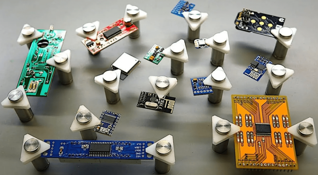
PCB miniaturization refers to the technical process of reducing the physical size of circuit boards while enhancing their functional density and electrical performance through advanced materials, design, and manufacturing processes. This concept is far from a simple size reduction; it involves a comprehensive innovation encompassing materials science, circuit design, and manufacturing technology. Miniaturized PCBs have now developed into various forms, including High-Density Interconnect (HDI) boards, Flexible Printed Circuits (FPCs), Rigid-Flex PCBs (R-FPCBs), and System-in-Package (SiP), to meet the needs of different application scenarios.
At the technical parameter level, PCB miniaturization is reflected in multiple dimensions: trace widths have shrunk from the traditional millimeter scale to the micrometer scale. Modern mobile phone PCBs can achieve trace widths of 5-10 micrometers, only about 1/10th to 1/8th the diameter of a human hair. Via diameters have also been reduced from 0.3mm to below 0.1mm, with over 100 microvias possible per square centimeter—a density five times greater than a decade ago. In terms of board thickness, ultra-thin PCBs can now be manufactured with thicknesses less than 0.1mm, while miniature circuit boards made from high-frequency materials like Rogers RO4350B can be as small as 0.8mm * 1.4mm, with a finished thickness of just 0.3mm.
Manufacturing miniaturized PCBs requires pushing beyond the limits of traditional processes. For small-size PCBs, the minimum dimensions can reach 1*1mm, with form tolerances needing to be controlled within ±0.05mm, and board outlines required to be smooth and burr-free. These precision requirements render traditional PCB production processes inadequate, necessitating advanced technologies such as Laser Direct Imaging (LDI), laser drilling, and vacuum lamination. It is these technological innovations that have made PCB miniaturization not only possible but also a continuous driver pushing electronic devices toward being smaller, more powerful, and more energy-efficient.
2. Factors Driving PCB Miniaturization
The rapid development of PCB miniaturization benefits from the combined push of multiple factors, with market demand, technological evolution, and industry competition constituting the primary drivers. The continuous innovation in consumer electronics is the foremost factor driving PCB miniaturization. From smartphones and wearable devices to foldable screen products, consumer demand for thin, light, and portable devices is endless. For instance, modern foldable phones internally use rigid-flex PCBs whose flexible areas feature copper layers only 12μm thick and substrate thicknesses of 25μm, yet can withstand over 100,000 bending cycles, ensuring product reliability over long-term use. This extreme pursuit of compact space forces PCB design toward higher density and smaller size.
Technological advancement is another major driving force. The semiconductor industry develops according to Moore’s Law, with chip process nodes continuously shrinking and integration levels steadily increasing. This requires supporting PCBs to provide higher pin density and finer traces. Concurrently, the application of AI-assisted design tools has significantly improved the design efficiency of complex miniature PCBs, including automatic layout, signal simulation, thermal expansion analysis, and real-time manufacturing feasibility checks, markedly shortening design cycles and reducing error rates. Companies like Siemens, through acquisitions, are integrating the entire workflow from design to manufacturing, further responding to the need for rapid development.
The explosive growth of emerging application fields has also injected strong momentum into PCB miniaturization. 5G communication base stations and terminal equipment require a large number of high-frequency miniature PCBs. For example, miniature boards measuring 0.8mm*1.4mm made from materials like Rogers RO4350B are specifically used for 5G communication components and SMD dielectric antennas. AI servers have far higher technical requirements for PCBs than traditional products, often incorporating 20 to 28 multilayer structures, significantly exceeding the 12 to 16 layers of traditional servers, with the PCB value per unit increasing to $8,000~$10,000. The electrification of automobiles, especially electric vehicles’ Battery Management Systems (BMS) and Advanced Driver-Assistance Systems (ADAS), relies on advanced PCBs to achieve higher performance and reliability.
Furthermore, environmental protection and sustainability requirements are also influencing the direction of PCB miniaturization. Tightening global environmental policies are prompting the industry to adopt halogen-free substrates, water-saving processes, and decomposable substrates. Companies like Germany’s Schweizer Electronic are introducing closed-loop water systems to reduce environmental impact. These environmental measures, while promoting sustainable industry development, also foster the application of new materials and processes, indirectly advancing the PCB miniaturization process.
3. Key PCB Miniaturization Technologies
Achieving PCB miniaturization relies on the collaborative development of several key technologies spanning materials, design, manufacturing, and packaging. High-Density Interconnect (HDI) technology is the core driver of PCB miniaturization, enabling higher wiring density within limited space through microvias and multilayer copper structures. HDI technology has allowed trace precision to leap from the “millimeter scale” to the “micrometer scale.” Modern high-end PCBs can achieve trace widths of 5-10μm, equivalent to laying 10-20 traces side-by-side across the width of a human hair. This precision leap relies on Laser Direct Imaging (LDI) technology, which offers a positioning accuracy of ±1μm—20 times higher than traditional exposure processes (±20μm)—and can control the error of a 10μm wide trace within ±0.5μm, ensuring adjacent traces do not short-circuit.
Advanced Drilling Technology is crucial for achieving high-density interconnects. Laser drilling technology uses picosecond lasers (pulse width one-trillionth of a second) to create holes in PCBs, enabling blind vias with diameters of 0.05mm and smooth, burr-free via walls—10 times more precise than mechanical drilling. These miniature vias are distributed densely like “capillaries”; modern high-end PCBs can distribute over 100 vias of 0.1mm diameter per square centimeter. Technologies like “blind vias” and “buried vias” (which only penetrate part of the layers) significantly reduce the occupation of surface space.
Material Innovation forms the foundation supporting PCB miniaturization. Ultra-high frequency applications require special high-frequency materials, such as Rogers RO4350B, which has a Dielectric Constant (Dk) of 3.48, making it very suitable for high-frequency applications like 5G communication components. Substrate thickness has also decreased from 0.2mm to 0.05mm (equivalent to the thickness of 5 sheets of A4 paper), using high-strength Polyimide (PI) or Liquid Crystal Polymer (LCP), which are both thin/light and heat resistant (above 120°C). Copper foil is also moving toward “ultra-thin,” with 12μm foil (thickness only 1/5th of a hair) becoming mainstream, and even 6μm foil appearing. Through electrolytic process optimization, the adhesion of ultra-thin copper foil reaches 1N/mm, ensuring it does not detach during soldering and bending.
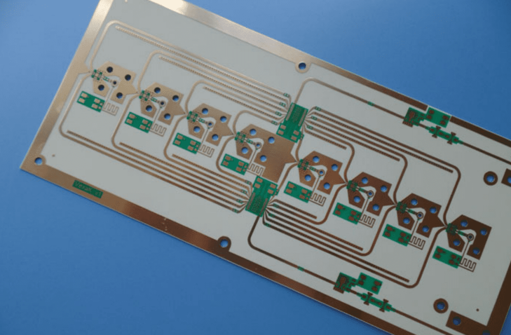
Table 1: Comparison of Key PCB Miniaturization Technologies
| Technology Category | Representative Technology | Key Technical Parameters | Main Application Fields |
|---|---|---|---|
| High-Density Interconnect | Laser Direct Imaging (LDI) | Trace width 5-10μm, Positioning accuracy ±1μm | Smartphones, High-end Communication Equipment |
| Micro Vias | Laser Drilling | Via diameter 0.05mm, Via density >100/cm² | Multilayer HDI Boards, Chip-Scale Packaging |
| Advanced Materials | Ultra-thin Substrate/Copper Foil | Substrate thickness 0.05mm, Copper foil thickness 6-12μm | Flexible Electronics, Wearable Devices |
| Integrated Packaging | System-in-Package (SiP) | Volume 0.5cm³, Delay reduced by 50% | Smartwatches, IoT Devices |
| Flexible Circuits | Rigid-Flex PCB | Bend cycles >100,000, Resistance change ≤3% | Foldable Phones, Medical Devices |
System-in-Package (SiP) Technology elevates PCB miniaturization to new heights. While chips, resistors, and capacitors are discrete components on traditional PCBs, SiP technology integrates multiple chips (e.g., CPU, memory, RF chip) and passive components within a single package, effectively realizing PCB functions at the chip level. The SiP module in a certain smartwatch, with a volume of only 0.5cm³, integrates the processor, sensors, and wireless communication functions, shrinking the size by 60% compared to traditional PCB solutions. Interconnects inside the SiP no longer rely on PCB traces but use gold wires (25μm diameter) or copper pillars (50μm height) for connections, reducing signal transmission distance from the centimeter scale to the millimeter scale and cutting delay by 50%.
Rigid-Flex PCB Technology provides miniaturization solutions for devices with special form factors. It consists of rigid areas (for mounting hard components like chips) and flexible areas (bendable polyimide substrate), connected precisely via laser cutting. This design allows the circuit to “bend,” adapting to the form factors of devices like foldable screen phones and smart bands, enabling three-dimensional wiring instead of traditional two-dimensional layouts, thereby saving significant space.
4. Challenges in PCB Miniaturization
The path to PCB miniaturization faces multiple challenges involving technical bottlenecks, cost pressures, supply chain stability, and talent shortages. The Physical Limits of Technology pose the primary challenge. As trace widths approach 5-10 micrometers, issues of signal integrity, power integrity, and electromagnetic compatibility become increasingly prominent. With trace spacing reduced to below 10 micrometers, the substrate’s insulation performance needs to be more excellent, requiring a stable Dielectric Constant (εr) between 3.8-4.2 to avoid crosstalk between traces. Simultaneously, the skin effect significantly impacts high-frequency scenarios; as signal transmission frequency increases, signal “distortion” caused by the skin effect becomes more severe, placing stringent demands on the selection of high-speed materials.
Thermal Management Challenges are particularly acute in miniaturized PCBs. High-density wiring leads to a sharp increase in power density, while the heat dissipation capacity within the tiny space is limited. When multiple chips operate in a compact space, localized overheating can cause performance degradation or even device failure. Traditional heat dissipation solutions are often difficult to implement in miniature PCBs, necessitating innovative thermal management strategies. For example, embedded component technology achieves system-level cost reduction and removal of heat sinks by embedding power chips within the board, but this requires the introduction of semiconductor-grade cleanrooms and IC processes.
Manufacturing Yield and Precision Control are significant obstacles to industrialization. The lamination misalignment for multilayer PCBs needs to be controlled within ±3μm (equivalent to 1/20th the diameter of a human hair); otherwise, miniature traces will misalign and short circuit. Vacuum lamination processes (temperature 180°C, pressure 1MPa), while allowing tight bonding between layers, are extremely sensitive to fluctuations in process parameters. Component placement accuracy requirements are equally astounding; placing a 01005 packaged resistor (0.4mm long, 0.2mm wide) requires an error of ≤±0.03mm, akin to placing a ping pong ball on a specified spot on a football field.
Material Selection and Compatibility issues limit the flexibility of miniaturized design. High-frequency and high-speed applications require specialized materials, such as high-end substrates from Rogers or Taconic, but these materials often have poor processability and are prone to defects like delamination and warping when mixed with FR-4. For instance, although PTFE laminates are suitable for millimeter-wave applications, their processing requires strict control of temperature and humidity (recommended 22°C±2°C), increasing manufacturing complexity and cost.
The complexity of Testing and Fault Diagnosis increases significantly with the degree of miniaturization. Traditional test probes struggle to contact miniature pads due to size reasons, while embedded components and stacked structures make fault location and repair nearly impossible. AI-driven Automatic Optical Inspection (AOI), X-ray solder joint inspection, and real-time thermal monitoring can partially address these issues, but the substantial investment required for these advanced inspection equipment raises overall production costs.
Supply Chain and Geopolitical Risks also cannot be ignored. PCB miniaturization relies on a stable supply of key materials like copper foil and resin. Furthermore, a shortage of specialized talent, particularly in high-frequency design and the application of AI-assisted tools, further constrains industry development. Additionally, startups in Taiwan and South Korea are facing insufficient high-density prototype capacity, with lead times extending to 7-9 weeks, creating obstacles to the widespread adoption of PCB miniaturization.
5. Overcoming PCB Miniaturization Challenges
Facing the multiple challenges of PCB miniaturization, the industry has developed a series of innovative solutions covering design methods, manufacturing processes, testing technologies, and collaborative models. Advances in Design and Simulation Tools provide prospective solutions for addressing miniaturization challenges. AI-assisted design tools are being widely applied in the PCB design process, including automatic layout, signal simulation, thermal expansion analysis, and real-time Design for Manufacturability (DFM) checks. These tools can not only automatically optimize component placement and routing paths but also predict potential defects during the manufacturing process, significantly shortening design cycles and reducing error rates. Siemens’ recent acquisition of Downstream Technologies aims to strengthen integration from design to manufacturing, responding to the need for rapid development.
Process Innovation is key to breaking through physical limits. The modified Semi-Additive Process (mSAP/SAP) pushes trace width/space below 10 micrometers, while laser drilling, back drilling, and high multilayer stacking processes support high-density interconnects. Back drill depth control is crucial for millimeter-wave circuits, requiring depth errors of less than 1 mil; laser back drilling processes can effectively control this parameter. For ultra-high layer count PCBs, Japan’s OKI has introduced a 124-layer PCB prototype specifically designed for AI semiconductor testing, enhancing signal integrity and bandwidth. On the architectural front, CoWoS packaging connects chips directly to the PCB by removing the ABF substrate, but this places extremely high demands on board surface flatness, dimensional stability, and manufacturing yield.
Advanced Material Development provides fundamental support for miniaturization. To meet the demands of high-speed applications, the use of low-profile copper foils is becoming increasingly widespread. For instance, both Mid Loss and Low Loss materials use Reverse-Treated Foil (RTF) as the standard copper foil. To achieve high-frequency and high-speed PCBs, high-end materials such as M9/PTFE resin, HVLP copper foil with Rz≤0.4μm, and low-loss quartz cloth become key to achieving 224G high-speed transmission. Halogen-free substrates, water-saving processes, and decomposable substrates are also being introduced, meeting environmental requirements without sacrificing performance.
Innovations in Testing and Quality Assurance technologies ensure the reliability of miniaturized PCBs. As layer counts and circuit density increase, traditional inspection methods become inadequate. The industry is adopting AI-driven Automatic Optical Inspection (AOI), X-ray solder joint inspection, and real-time thermal monitoring to enhance quality control capabilities. For high-speed interfaces, eye diagram testing has become an important verification method; a 10Gbps signal requires an eye height >200mV, eye width >70% UI, and the test oscilloscope must support PAM4 modulation analysis.
Supply Chain Optimization and Talent Cultivation represent the soft power supporting the industry’s sustainable development. Facing material shortages and geopolitical risks, leading companies are responding through diversified sourcing and strategic inventory management. Simultaneously, collaboration between industry and universities is strengthening to cultivate professionals skilled in high-frequency design, AI-assisted tool application, and advanced materials knowledge, addressing the talent shortage.
The Collaborative Design Model breaks down traditional design silos. PCB designers, chip designers, packaging engineers, and system architects collaborate early to jointly optimize the overall solution. This collaborative approach ensures that PCB miniaturization is not conducted in isolation but is closely integrated with Signal Integrity (SI) and Electromagnetic Compatibility (EMC) design, achieving system-level optimization. The orthogonal backplane solution, which requires M9 or PTFE low-loss materials to meet 224G SerDes transmission needs, is a successful case of collaborative design.
6. Common Miniature Circuit Board Applications
Miniaturized PCB technology has penetrated almost all electronic application fields, from consumer electronics to high-end industrial equipment, and its application scope continues to expand. Consumer Electronics is the most widespread application area for miniature PCBs. Smartphones are a typical example, where their mainboards use HDI technology with trace width/space refined to 5-10 micrometers and via density exceeding 100 per square centimeter, integrating processors, memory, communication modules, and various sensors within an extremely small space. Foldable phones further utilize rigid-flex PCB technology; the flexible areas have copper layers only 12μm thick and substrate thicknesses of 25μm, capable of withstanding over 100,000 bends, ensuring reliable operation in the hinge area. Smartwatches and health monitoring devices widely use System-in-Package (SiP) technology. For instance, the SiP module in a certain smartwatch has a volume of only 0.5cm³ yet integrates the processor, sensors, and wireless communication functions, shrinking the size by 60% compared to traditional PCB solutions.
Communication Infrastructure heavily relies on miniaturized PCB technology. 5G base stations require a large number of high-frequency PCBs, such as miniature boards made from Rogers RO4350B material, sized at just 0.8mm*1.4mm, specifically used for 5G communication components and SMD dielectric antennas. High-speed optical modules also require precise miniature PCBs to support 800G乃至1.6T transmission rates. Companies like Avary Holding’s SLP products have entered the 800G/1.6T optical module supply chain and are developing 3.2T products. These applications require PCB materials to have a stable Dielectric Constant (Dk) and low Dissipation Factor (Df) to ensure signal transmission quality.

Automotive Electronics has become an important market for miniature PCBs. The Battery Management Systems (BMS) of new energy vehicles rely on highly reliable PCBs to accurately monitor and manage battery status. Advanced Driver-Assistance Systems (ADAS) use numerous sensors and control systems requiring high-performance miniature PCBs to process massive data. The vibration, temperature variations, and electromagnetic interference in automotive environments demand PCBs with higher reliability and stability. Rigid-flex boards perform excellently in this field as they can better absorb vibrations, reduce connector usage, and improve system reliability.
Computing and Data Centers are core application areas for high-end miniaturized PCBs. AI servers have far higher technical requirements for PCBs than traditional products, typically containing 20 to 28 multilayer structures, significantly exceeding the 12 to 16 layers of traditional servers. Companies like Shennan Circuits, as core global suppliers of high-end PCBs, ranked first globally in revenue for the AI/HPC segment in Q1 2025, deeply participating in high-end AI server projects like NVIDIA’s GB200. High-speed switches also require high-performance PCBs. Wushengyuan recently reported outstanding performance in high-speed network switch-related products, with a year-on-year growth of +161.46% in H1 2025. Its 800G switch products have achieved volume shipment, and it is proactively laying out next-generation 1.6T switch technology.
Table 2: Main Application Areas and Technical Requirements for Miniature PCBs
| Application Area | Representative Products | Key Technical Requirements | Common PCB Types |
|---|---|---|---|
| Consumer Electronics | Smartphones, Wearables | Trace width 5-10μm, Via diameter ≤0.1mm | HDI, Rigid-Flex PCB |
| Communication Equipment | 5G Base Stations, Optical Modules | High-frequency materials (Dk=2.2-3.48), Low loss | Rogers HF Boards |
| Automotive Electronics | ADAS, BMS | High reliability, High temp resistance, Vibration resistance | Rigid-Flex PCB, Heavy Copper Boards |
| Computing Equipment | AI Servers, Switches | 20-28 layers, High-speed materials, Back drilling | High-Speed Multilayer Boards |
| Medical Devices | Implantable Devices, Diagnostic Equipment | Ultra-high reliability, Miniaturization, Biocompatibility | Flexible Boards, HDI Boards |
In the Medical Electronics field, miniaturized PCBs are opening new possibilities. Implantable medical devices like pacemakers and neurostimulators require extremely miniaturized and highly reliable circuit boards whose size and thickness must be minimized to fit the limited space inside the human body. Flexible circuits excel in this field as they can adapt to irregular shapes and withstand mechanical stress from body movements. Diagnostic equipment like portable ultrasound machines and continuous glucose monitoring systems also extensively use miniaturized PCBs to integrate signal acquisition, processing, and transmission functions within a limited space.
In Industrial and IoT applications, miniaturized PCBs support the process of device intelligence and connectivity. Industrial sensors, automation control modules, and smart meters require robust and compact circuit solutions. VIA Technologies’ Mobile-ITX module, with a board size of 6cm x 6cm, is one of the most compact computer module form factor standards currently on the market, widely used in industrial automation, robotics, transportation sectors, and handheld devices. IoT node devices need to balance miniaturization with low power consumption, typically adopting highly integrated PCB solutions to achieve sensing, computing, and communication functions within a tiny footprint.
7. What is the Future of PCB Miniaturization?
PCB miniaturization technology will continue to evolve, with various innovative technologies and trends collectively shaping its future development direction. Deep Integration with Advanced Packaging will become a core path for PCB miniaturization. With the maturation of 2.5D/3D packaging technologies like Chip on Wafer on Substrate (CoWoS), PCBs are evolving from mere connectors into functional integration platforms. CoWoS packaging connects chips directly to the PCB by removing the ABF substrate, significantly increasing integration density but placing extremely high demands on board surface flatness, dimensional stability, and manufacturing yield. Leading domestic companies like Shennan Circuits are deeply involved in this field, actively developing high-end PCB products suitable for advanced packaging.
Breakthroughs in New Materials will push the performance boundaries of PCB miniaturization. As signal transmission rates move toward 224G and beyond, the demand for low-loss materials becomes increasingly urgent. High-end materials such as M9/PTFE resin, HVLP copper foil with Rz≤0.4μm, and low-loss quartz cloth will be key to achieving 224G high-speed transmission. Emerging materials like graphene and nanomaterials are also under research, promising to further enhance the conductivity, thermal management capability, and mechanical strength of PCBs. Eco-friendly materials are also receiving significant attention; halogen-free substrates and decomposable substrates will gradually become popular, promoting the industry’s green transformation.
Smart Manufacturing Technologies will fundamentally change the production methods of PCB miniaturization. The application of Industrial Internet, Big Data, and Artificial Intelligence in PCB manufacturing will deepen, enabling intelligent management and control of the production process. AI-driven Automatic Optical Inspection (AOI), X-ray solder joint inspection, and real-time thermal monitoring will become standard configurations, greatly improving product quality and consistency. Smart production equipment can monitor production parameters in real-time, automatically adjust production processes, and improve production efficiency and product quality stability.
3D Printing and Additive Manufacturing technologies have the potential to reshape the PCB manufacturing process. 3D printing is accelerating prototyping speeds and supporting special外形. As material performance and precision improve, it may enable more complex three-dimensional circuit structures in the future, breaking through the limitations of traditional two-dimensional wiring. This will provide greater design freedom for electronic products, achieving better integration of form and function.
Expansion of Application Fields will inject continuous momentum into PCB miniaturization. The explosive growth of AI and Edge Computing places higher demands on miniaturized, high-performance PCBs. According to Prismark projections, the global PCB output value is expected to reach $94.661 billion by 2029, with a CAGR of 5.2% from 2024 to 2029. The server/storage segment shows the strongest growth, with a projected CAGR of 11.6%. Trends such as automotive electrification, medical device miniaturization, and the proliferation of wearable devices will also continue to drive PCB miniaturization technology forward.
Addressing Technical Challenges will guide future research directions. As trace width/space further shrinks, issues of signal integrity, power integrity, and thermal management will become more prominent. The orthogonal backplane solution, requiring M9 or PTFE low-loss materials to meet 224G SerDes transmission, and embedded component technology, which achieves system-level cost reduction and heat sink removal by embedding power chips within the board, represent cutting-edge directions for addressing miniaturization challenges.
China’s PCB industry will play an increasingly important role in the future global landscape. According to Prismark data, the PCB output value in Mainland China was $41.213 billion in 2024, accounting for 56% of the global total, and is projected to reach $49.704 billion by 2029. In the future, Chinese PCB enterprises will focus more on product added value, transitioning from low-value-added standard PCB products to high-value-added, high-end, and customized products by increasing technical content, optimizing product structure, and enhancing brand influence.
Summary
PCB miniaturization is an ongoing technological revolution that has fundamentally altered the form and function of electronic products and reshaped the landscape of multiple industries. Evolving from initial size reduction to today’s functional integration, PCB miniaturization has developed into a complete innovation system encompassing materials science, circuit design, manufacturing processes, and testing technologies. As trace widths have moved from the millimeter scale to the micrometer scale, via density has increased severalfold, and board thickness has continuously decreased, PCBs have achieved unprecedented functional density within limited space, supporting the vigorous development of numerous fields such as smartphones, wearable devices, 5G communication, AI servers, and automotive electronics.
The future of PCB miniaturization will be more multi-dimensional and high-performance. Deep integration with advanced packaging, the application of new materials, the widespread adoption of smart manufacturing technologies, and the introduction of innovative processes like 3D printing will further propel PCB miniaturization technology forward. With the maturation of emerging technologies like AI, IoT, and Edge Computing, the demand for miniaturized, high-performance PCBs will continue to grow, making value enhancement the core goal of industry development. As the world’s largest PCB production base, China is at a critical juncture transitioning from scale expansion to value leap, poised to occupy a more important position in the future global industrial landscape.
Looking ahead, PCB miniaturization technology will continue to follow the development path of “smaller, denser, stronger,” but will also pay more attention to the comprehensive balance of performance, reliability, and cost. As technological boundaries are continuously broken, PCBs—this “invisible foundation” of the electronics industry—will continue to play a key role, providing solid support for innovation and upgrading in the global electronics industry. The manufacturers who stand out in the fierce competition will undoubtedly be those that actively embrace new technologies, invest in talent cultivation, and maintain process flexibility.


0 Comments