
Introduction
In modern high-performance electronic systems, Power Distribution Network (PDN) design has become a critical factor determining system stability and performance. As chip process sizes continue to shrink and supply voltages decrease further, the noise tolerance of power supply systems is tightening, and requirements for voltage fluctuations have become extremely stringent. For example, in a processor with a core voltage of only 0.8V, the allowable voltage ripple may not exceed ±2%, which is 16mV. Simultaneously, the instantaneous current demands of high-speed digital circuits and RF modules can reach tens or even hundreds of amperes. Any power integrity issue can lead to signal timing errors, excessive electromagnetic interference (EMI), or even system functional failure.
The PDN is the complete power delivery path from the power supply module to the chip pins, including components such as the Voltage Regulator Module (VRM), decoupling capacitors, power/ground planes, and vias. An excellent PDN design provides stable, clean supply voltage to the load under all operating conditions, ensuring optimal system performance across various operating frequencies. This article will start with the basic concepts of PDN, systematically introduce its key components, design, challenges, and best practices, providing engineers with a complete and practical PDN design guide.
1. What is PDN Design?
Power Distribution Network (PDN) design refers to the systems engineering involved in planning and optimizing the entire electrical energy transmission path from the power source to the load chip on a printed circuit board (PCB). Its primary goal is to provide a stable and clean supply voltage to integrated circuits under all operating conditions—including static, dynamic, and transient load variations. As digital system clock frequencies increase and supply voltages decrease, the complexity of PDN design has grown significantly, with its performance directly impacting system power efficiency, signal integrity, and electromagnetic compatibility (EMC).
From a system perspective, the PDN is a complex network containing multiple frequency components. In the low-frequency range (typically below 1MHz), the power converter (VRM) dominates the response; in the mid-frequency range (1MHz to several hundred MHz), various decoupling capacitors play the primary role; and in the high-frequency range (above several hundred MHz), the distributed parameters of the power/ground planes and package parasitics become critical. For example, a high-performance FPGA might have a current demand that instantly jumps from tens of milliamps (idle state) to tens of amperes (full-load operation) during normal operation. Such drastic current changes induce voltage noise across the PDN impedance. If the PDN impedance is too high, it can cause the supply voltage to exceed the chip’s allowable operating range.
2. Key PDN Components
The PDN consists of several key components, each responsible for impedance control within a specific frequency range. Understanding the characteristics of these components and their interactions within the PDN is fundamental to successful design.
Voltage Regulator Module (VRM)
The VRM is the source of the PDN, responsible for converting the board-level input voltage (e.g., 12V or 5V) to the low voltage required by the chip (e.g., 1.0V or 0.8V). Modern switching regulators typically have a bandwidth of 500kHz to 1MHz, enabling them to respond effectively to low-frequency current demands. However, due to control loop delays and the presence of output inductors, the VRM’s ability to respond to high-frequency current changes is limited; generally, its impedance increases significantly above approximately 1MHz. For example, a typical VRM might have an impedance of 2mΩ at 10kHz, but this could rise to over 20mΩ at 1MHz.
Decoupling Capacitors
Decoupling capacitors are the core of PDN design. They are strategically placed on the PCB to compensate for the VRM’s inadequacies at high frequencies. Based on their frequency characteristics, decoupling capacitors can be categorized as follows:
- Bulk Capacitors: Typically electrolytic or tantalum capacitors with values ranging from 10μF to 1000μF, effective from DC to a few hundred kHz. Their main role is to provide low-frequency current buffering and stabilize the VRM output.
- Ceramic Capacitors: Capacitance values range from 100nF to 10μF, effective from a few hundred kHz to several tens of MHz. Due to their low Equivalent Series Resistance (ESR) and low Equivalent Series Inductance (ESL), ceramic capacitors are the workhorses for mid-frequency decoupling.
- Small-Value High-Frequency Capacitors: Values between 1nF and 100nF, specifically used to suppress high-frequency noise above several hundred MHz. They are typically placed very close to the chip’s power pins to minimize parasitic inductance.
Table: Key PDN Components and Their Characteristics
| Component Type | Typical Value/Parameter | Effective Frequency Range | Primary Function | Parasitic Parameter Impact |
|---|---|---|---|---|
| VRM | Output Inductor 0.2~1μH | DC ~ 1MHz | Provides base DC voltage & LF response | Loop delay, output inductance |
| Electrolytic Capacitor | 10μF ~ 1000μF | DC ~ 100kHz | LF energy storage, stabilizes VRM | High ESR (10~100mΩ) |
| Ceramic Capacitor | 100nF ~ 10μF | 100kHz ~ 50MHz | Mid-frequency decoupling, suppresses MF noise | Low ESR (<10mΩ) |
| High-Freq Capacitor | 1nF ~ 100nF | 50MHz ~ 1GHz | Suppresses HF noise, provides fast current response | Very low ESL (<0.5nH) |
| Power/Ground Plane | Spacing 2~8mil | 10MHz ~ 1GHz+ | Provides low-impedance return path, distributed capacitance | Plane resonance, characteristic impedance |
3. PDN Design Process Steps
A systematic PDN design process is crucial for ensuring power integrity. The following outlines the detailed steps of a typical PDN design cycle, covering everything from target setting to verification.
Step 1: Determine Target Impedance
The target impedance is the core metric of PDN design. As mentioned earlier, it is determined by the supply voltage, allowed ripple, and maximum transient current. In practical design, engineers must carefully analyze the chip’s datasheet and operating modes to determine the worst-case current demand. For example, a high-performance processor might specify a maximum transient current of 25A, a supply voltage of 0.9V, and an allowed ripple of ±3%. The target impedance is calculated as:
Z_{target} = \frac{0.9V \times 3\%}{25A} = 1.08m\Omega
This target impedance must be met across the frequency range from DC to very high frequencies (typically 5-10 times the chip’s highest clock frequency).
Step 2: Frequency Domain Impedance Analysis
Based on the target impedance, the designer must plan the PDN’s impedance profile in the frequency domain. This includes:
- Low-Frequency Range (DC ~ 100kHz): Primarily relies on VRM performance, ensuring its output impedance is below the target value.
- Mid-Frequency Range (100kHz ~ 50MHz): Provides a low-impedance path through a combination of bulk and ceramic capacitors.
- High-Frequency Range (above 50MHz): Utilizes small-value high-frequency capacitors and the distributed capacitance of power/ground planes to control impedance.
Using simulation tools (e.g., ANSYS SIwave, Keysight ADS), this impedance profile can be modeled and optimized to ensure no significant resonant peaks exceed the target impedance.
Step 3: Decoupling Capacitor Selection and Placement
Selecting appropriate decoupling capacitors and determining their placement is the most practical aspect of PDN design. Capacitor selection must consider not only capacitance value but also parasitic parameters (ESR and ESL). For example, a 100nF, 0402 package ceramic capacitor typically has an ESL of about 0.5nH and a self-resonant frequency of approximately 23MHz. Beyond the self-resonant frequency, the capacitor becomes inductive, and its decoupling effectiveness drops sharply.
Capacitor placement is equally critical. High-frequency decoupling capacitors should be placed as close as possible to the chip’s power pins to minimize loop inductance. A rule of thumb is that even an extra 1mm of trace length can add more than 1nH of inductance, severely impacting high-frequency performance. For BGA-packaged chips, it is generally recommended to place vias under the ball grid array for direct connection to power and ground planes, and to place high-frequency capacitors on the opposite side of the board.
Step 4: Power Plane Design and Optimization
Power plane design requires consideration of several aspects:
- Plane Shape and Segmentation: Rational plane segmentation can isolate noise-sensitive power domains (e.g., analog and digital supplies), but improper segmentation can increase return path length, leading to higher impedance.
- Via Placement: The number and location of power vias should ensure uniform current density and avoid local hotspots. Typically, at least 1-2 vias are needed per ampere of current.
- Plane Resonance Control: Use simulation tools to analyze the plane’s resonant modes. If necessary, add matching resistors or ferrite beads to suppress resonance.
Step 5: System Simulation and Verification
After PCB layout completion, use professional Power Integrity (PI) simulation tools for full-board PDN simulation. Simulations should cover all important operating states, including worst-case current loads and temperature conditions. Through simulation, potential impedance peaks, resonance issues, and areas with excessive voltage drop can be identified, guiding layout optimization.
4. Challenges in PDN Design
PDN design faces multiple challenges stemming from the continuous increase in power consumption, speed, and integration density of modern electronic systems.
Transient Current Demands
The power consumption patterns of modern processors and ASICs are highly dynamic, potentially switching from low-power states to full-load operation within nanoseconds, causing huge current changes (di/dt). For example, a 5G baseband chip might generate a current slew rate (di/dt) of 15A/ns during operation. According to the formula ( V = L \cdot di/dt ), even with just 1nH of PDN path inductance, this produces 15mV of voltage noise. If multiple loads switch simultaneously, the accumulated noise can easily exceed the allowed ripple range.
Resonance and Anti-Resonance
The PDN network, composed of numerous capacitive and inductive elements, inevitably forms resonant circuits. When decoupling capacitors of different values are connected in parallel, they can create anti-resonance peaks at specific frequencies, causing the impedance at those frequencies to be much higher than that of the individual components. For example, connecting a 10μF capacitor (self-resonant at 2MHz) in parallel with a 100nF capacitor (self-resonant at 15MHz) might produce a noticeable anti-resonance peak around 8MHz, increasing the impedance several-fold. Eliminating these peaks requires careful capacitor value selection or the use of capacitors with different ESR values to dampen the resonance.
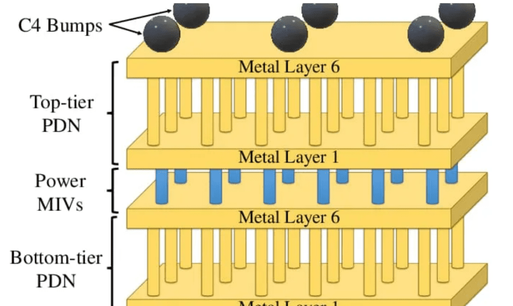
Package and Board-Level Co-Design
The PDN characteristics of the chip package itself significantly impact overall performance. Power routing, bond wires, or C4 bumps within the package introduce parasitic inductance and resistance. For instance, a 1mm long bond wire might introduce 1nH of inductance, generating significant voltage drop during high-speed current transients. Therefore, excellent PDN design must co-consider package and board-level characteristics, involving joint simulation and optimization. However, package parameters are usually provided by the chip supplier, and designers may not have access to complete models, adding uncertainty to the design.
Space and Cost Constraints
In miniaturized devices (e.g., smartphones, IoT nodes), PCB area is extremely limited, preventing the placement of a large number of decoupling capacitors. Simultaneously, high-performance capacitors with low ESR/ESL are more expensive and might be reduced in cost-sensitive consumer products due to cost pressures. Designers must make fine trade-offs between performance, size, and cost, for example, by adopting new packaging technologies with integrated decoupling functionality (e.g., embedded substrate capacitors) or optimizing stack-up design to enhance plane capacitance.
Table: Main PDN Design Challenges and Countermeasures
| Challenge Type | Specific Manifestation | Potential Impact | Countermeasures |
|---|---|---|---|
| High Transient Current | di/dt > 10A/ns | Excessive voltage sag, timing errors | Optimize capacitor combination, reduce path inductance, use faster VRMs |
| Resonance & Anti-Resonance | Sharp peaks in impedance curve, exceeding target Z | Noise amplification at specific freq., instability | Optimize capacitor values, use damping resistors, adjust plane structure |
| Package-Board Co-Design | Package parasitic inductance increases HF impedance | Degraded voltage quality at chip side | Joint simulation, obtain complete models, optimize package selection |
| Space & Cost Limits | Limited PCB area, insufficient space for capacitors | High-frequency performance not met | Use high-frequency materials, optimize stack-up, use integrated capacitor tech |
| Multi-Domain Interference | Digital noise coupling into analog/RF supplies | Reduced SNR, increased communication BER | Rational plane segmentation, use isolation techniques, optimize grounding |
5. PDN Design Guidelines and Best Practices
Based on the aforementioned challenges, the following PDN design guidelines and best practices can help engineers achieve robust power integrity.
Adopt a Frequency-Band Decoupling Strategy
Effective PDN design needs to cover a broad frequency band from DC to very high frequencies, and a single type of capacitor cannot meet the full-band需求. Therefore, a frequency-band decoupling strategy should be employed, using a combination of capacitors with different values and types. For example:
- Low-Frequency Band (DC ~ 1MHz): Use VRM and bulk capacitors (e.g., 100μF electrolytic capacitors).
- Mid-Frequency Band (1MHz ~ 100MHz): Use multiple values of ceramic capacitors (e.g., 10μF, 1μF, 0.1μF).
- High-Frequency Band (above 100MHz): Use small-value ceramic capacitors (e.g., 1nF, 100pF) and power-ground plane capacitance.
This combination ensures that across the entire frequency band, capacitors are at or near their resonant frequency, providing low-impedance paths.
Minimize Loop Inductance
Parasitic inductance in the PDN is the main limiting factor for high-frequency performance. To minimize inductance, take the following measures:
- Use Small Package Capacitors: Capacitors in 0201 or 01005 packages have lower ESL than those in 0402 or 0603 packages.
- Optimize Via Layout: Provide multiple parallel ground and power vias for each decoupling capacitor to reduce via inductance.
- Shorten Return Paths: Ensure the physical path between the decoupling capacitor and the chip pin is minimal; place power and ground vias as close as possible.
For example, an optimized decoupling capacitor layout can reduce loop inductance from 2nH to 0.5nH, thereby doubling the resonant frequency and greatly improving high-frequency performance.
Power Plane Optimization
Power plane design should follow these principles:
- Use Thin Dielectric Layers: Using thin dielectric layers (e.g., 2mil or less) between power and ground planes increases interplane capacitance, aiding high-frequency decoupling. For instance, with an FR-4 dielectric (εr=4.2) and a thickness of 2mil, the capacitance per unit area is approximately 250pF/cm².
- Avoid Plane Splits: Where possible, avoid splitting the power plane to provide a continuous low-impedance return path. If splits are unavoidable (e.g., for analog and digital supply isolation), ensure signal traces do not cross the split gap to avoid increasing return path inductance.
- Control Plane Resonance: Suppress resonance by adding lossy materials (e.g., magnetic films) or using irregularly shaped planes.
Collaborative Simulation and Verification
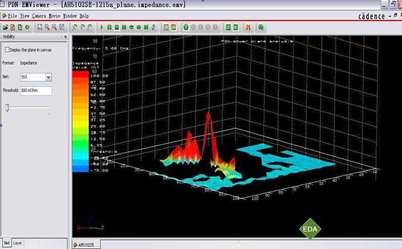
PDN design should not be conducted in isolation but should be coordinated with Signal Integrity (SI) and Electromagnetic Compatibility (EMC) design. Using advanced simulation tools (e.g., ANSYS HFSS, Cadence PowerSI) for co-simulation allows assessment of the PDN’s overall impact on system performance. Furthermore, during the hardware verification stage, using a Vector Network Analyzer (VNA) to measure the PDN impedance profile and using an oscilloscope to measure power supply ripple are essential steps to ensure the design meets targets.
Consider Thermal Effects and Aging
Capacitor performance changes with temperature and operating time. For example, the ESR of tantalum capacitors can increase significantly with rising temperature, and the capacitance of ceramic capacitors can vary with DC bias voltage. In harsh environments (e.g., automotive or industrial applications), designers must consider these factors and select components suitable for the temperature range with stable aging characteristics.
6. PDN Design Frequently Asked Questions (FAQ)
Q: How many decoupling capacitors are sufficient?
A: The number of decoupling capacitors depends on the PDN target impedance, capacitor characteristics, and operating frequency. A systematic approach involves calculating the total capacitance requirement based on the impedance needs and considering frequency coverage. For example, if the target is an impedance below 2mΩ at 100MHz, and the capacitors used have an ESL of 0.5nH, the required total capacitance can be estimated by ( Z = \sqrt{ESL/C} ), yielding C ≈ 12.5nF. However, in practical design, capacitor distribution and resonance must also be considered. It is generally recommended to use simulation tools for precise calculation.
Q: How to choose capacitor values?
A: When selecting capacitor values, ensure the self-resonant frequencies of adjacent value capacitors overlap to avoid anti-resonance peaks. A common value sequence is 10μF, 1μF, 0.1μF, 0.01μF, whose self-resonant frequencies roughly cover 2MHz, 5MHz, 15MHz, 50MHz. Additionally, refer to the chip manufacturer’s recommendations and adjust based on actual simulation results.
Q: When should ferrite beads be used?
A: Ferrite beads are used to isolate different power domains (e.g., analog and digital supplies) or suppress noise at specific frequencies. However, beads introduce DC Resistance (DCR) and have saturation current limits, which can cause unwanted voltage drop. Therefore, use ferrite beads only when necessary, and carefully evaluate their DCR, current rating, and impedance-frequency characteristics.
Q: How to measure PDN performance?
A: PDN performance can be measured using the following methods:
- Impedance Measurement: Use a VNA with the injection method to measure the PDN impedance profile.
- Ripple Measurement: Use a high-resolution oscilloscope and low-noise probe to measure voltage ripple at the chip’s power pin.
- Dynamic Response Test: Verify the PDN’s response to rapid current changes through load transient tests.
Q: How do plane capacitance and discrete capacitors work together?
A: Plane capacitance provides distributed decoupling capability in the high-frequency range, typically effective from tens of MHz to GHz. Discrete capacitors are responsible for the low to mid-frequency range and provide local charge sources. The two work together to ensure low impedance across the entire frequency band. During design, optimize plane spacing and dielectric materials through simulation to maximize the benefits of plane capacitance.
Conclusion
Power Distribution Network (PDN) design is the cornerstone of achieving high-performance electronic systems. With advancing chip technology and increasing system complexity, the challenges of PDN design are becoming more severe, requiring engineers to possess profound theoretical knowledge and rich practical experience. This article has systematically elaborated on the basic concepts, key components, design process, main challenges, and best practices of PDN, providing engineers with a comprehensive design guide.
Excellent PDN design is not merely about selecting the right capacitors or optimizing layout; it is a systems engineering task that requires collaborative optimization across the entire chain from chip and package to board level. Through clear target impedance setting, scientific frequency band planning, careful component selection and placement, and adequate simulation verification, engineers can build a robust and efficient PDN, providing a solid guarantee for the overall performance and reliability of the system. In the future, with further reduction in supply voltages and continuous increase in system power consumption, PDN design will remain a key and cutting-edge area in electronic engineering.


0 Comments