
Introduction
Through-hole assembly, also known as Through-Hole Technology (THT), represents one of the foundational methodologies in electronic component mounting, where component leads are inserted through pre-drilled holes in printed circuit boards (PCBs) and soldered to pads on the opposite side to establish both mechanical and electrical connections. This technology emerged in the 1950s as a revolutionary advancement over point-to-point wiring, dominating electronic manufacturing until the rise of surface mount technology (SMT) in the late 1980s. Despite the current prevalence of SMT, through-hole assembly maintains critical importance in applications requiring superior mechanical strength, high power handling, and enhanced reliability under stressful environmental conditions .
The significance of through-hole technology persists in modern electronics manufacturing due to its unparalleled reliability for specific applications. While SMT excels in miniaturization and high-density packaging, through-hole assembly provides robust connections essential for components subjected to mechanical stress, high power, or thermal cycling. Industries such as aerospace, automotive, automotive, industrial controls, and power electronics continue to rely on through-hole technology for connectors, transformers, large capacitors, and other components where permanent, durable connections are paramount. The technology’s relative simplicity also makes it ideal for prototyping, education, and applications where automated assembly may not be economically feasible .
1 What is Through-Hole Assembly?
Through-hole assembly is a method of electronic component mounting where component leads are inserted through plated holes in a printed circuit board and soldered to pads on the opposite side. This technology creates robust mechanical bonds and reliable electrical connections that withstand environmental stress better than surface-mount alternatives. The fundamental distinction between through-hole and surface-mount technology lies in the mechanical connection approach: while SMT components mount directly onto PCB pads, through-hole components physically penetrate the board substrate, creating anchors that provide superior resistance to mechanical strain, vibration, and thermal cycling .
The through-hole assembly process encompasses several key stages, beginning with component preparation (including lead forming), followed by insertion, and culminating in soldering. Components are categorized by their lead configuration: axial leads (extending from opposite ends of a cylindrical component) and radial leads (extending from the same side). Additionally, through-hole technology accommodates multi-lead devices such as single in-line packages (SIPs) and dual in-line packages (DIPs) for integrated circuits. The soldering process typically employs wave soldering systems where boards pass over a molten solder wave, though selective soldering and hand soldering are also used for specialized applications .
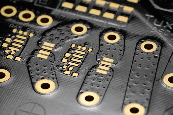
Through-hole components exhibit distinct physical characteristics optimized for their insertion methodology. Lead diameters typically range from 0.5mm to 0.8mm, with corresponding hole sizes providing 0.2mm to 0.3mm clearance for manual insertion or 0.3mm to 0.4mm for automated processes. Standard lead spacing follows metric or imperial systems, with common pitches of 2.54mm (0.1 inches) or multiples thereof. These standardized dimensions ensure compatibility across components and facilitate automated assembly processes .
2 Advantages and Disadvantages of Through-Hole Assembly
Through-hole assembly offers distinct advantages that ensure its continued relevance in specific electronic applications. The technology’s foremost strength lies in its exceptional mechanical robustness. Components secured through board holes withstand substantially greater physical stress than surface-mounted equivalents, with mechanical connection strengths typically 3-5 times greater than SMT connections. This makes through-hole technology ideal for connectors, switches, and other components subject to frequent mating cycles or mechanical manipulation. The through-board anchoring also provides superior resistance to vibration and shock, critical in automotive, aerospace, and industrial applications where reliability under stress is paramount .
The power handling capability of through-hole assembly represents another significant advantage. The physical mass of through-hole leads and their direct connection through the board substrate enables better heat dissipation than SMT alternatives. Through-hole components routinely handle currents of 10A or higher without specialized cooling, making them indispensable for power supply units, motor controllers, and power conversion systems. The technology also facilitates easier visual inspection of solder joints, simplifying quality control and rework processes. This accessibility makes through-hole particularly valuable for prototyping, debugging, and educational applications where frequent component changes may be necessary .
However, through-hole technology presents several limitations that restrict its application in modern electronics. The most significant drawback is reduced board space efficiency. Through-hole components consume substantially more real estate on both sides of the PCB, with typical footprint requirements 3-10 times greater than equivalent SMT components. This limitation becomes critical in miniaturized devices where internal space constraints dictate component selection. Additionally, the requirement for drilled holes consumes valuable routing space on inner layers of multi-layer boards, further reducing design flexibility compared to SMT approaches .
The manufacturing efficiency of through-hole assembly also lags behind SMT for high-volume production. The multi-step process—drilling, insertion, and soldering—requires more time and equipment than streamlined SMT lines. Automated through-hole insertion machines typically place 10,000-30,000 components per hour, significantly slower than high-speed SMT placers exceeding 100,000 components per hour. This speed differential, combined with higher material costs (drilled PCBs, typically larger components) makes through-hole assembly less economically attractive for high-volume consumer products where miniaturization and cost minimization are primary concerns .
Table: Through-Hole vs. Surface Mount Technology Comparison
| Parameter | Through-Hole Technology | Surface Mount Technology |
|---|---|---|
| Board Space Utilization | Lower (requires both sides) | Higher (single-side possible) |
| Mechanical Strength | Superior (through-board anchor) | Good (dependent on solder joint) |
| Power Handling | Excellent (better thermal dissipation) | Limited (requires thermal management) |
| Assembly Speed | Slower (multi-step process) | Faster (streamlined process) |
| Repairability | Easier (accessible joints) | More challenging (miniature joints) |
| High-Frequency Performance | Limited (longer leads create inductance) | Superior (shorter signal paths) |
3 Through-Hole Assembly Components
Through-hole components are characterized by their leaded configuration designed for insertion through PCB holes. These components fall into two primary categories based on lead orientation: axial lead components feature leads extending from opposite ends of a cylindrical body, aligned along the component’s central axis. Common examples include resistors, diodes, and certain capacitors. This configuration allows components to span between holes, potentially without additional support. Radial lead components feature parallel leads protruding from the same side of the component body, enabling perpendicular mounting to the board surface. This configuration includes electrolytic capacitors, inductors, and connectors, offering space savings in the horizontal dimension at the expense of increased vertical profile .
Component packaginging follows standardized dimensional systems to ensure interoperability across manufacturers. The lead diameter for most through-hole components ranges from 0.5mm to 0.8mm, with power components extending to 1.0mm or larger. The lead spacing (distance between lead centers) typically adheres to standardized increments, with 2.54mm (0.1 inches) being most common, and multiples thereof for multi-pin devices. Component bodies vary significantly based on function and rating, with resistor and capacitor dimensions standardized by power handling capability or capacitance/voltage rating respectively .
Multi-lead through-hole components include single in-line packages (SIPs) and dual in-line packages (DIPs). SIPs contain a single row of pins with standard spacing, commonly used for resistor networks, sensor arrays, and certain integrated circuits. DIPs feature parallel pin rows on opposite sides, predominantly for integrated circuits with pin counts ranging from 8 to 64 pins. These standardized packages facilitate automated insertion and ensure compatibility across manufacturing systems. Additionally, specialized through-hole components include connectors, switches, relays, and large capacitors whose mechanical requirements justify the through-hole approach .
Mechanical components represent a significant through-hole application category where physical robustness is paramount. Terminal blocks, connectors, and electromechanical relays benefit from the enhanced mechanical fixation provided by through-board mounting. Similarly, large electrolytic capacitors and transformers utilize through-hole technology for both electrical connection and physical stability. These components often incorporate mounting features such as slots, flanges, or retention clips that complement the soldered connections, providing additional mechanical security against vibration or accidental dislodgement .
4 Through-Hole PCB Assembly Technology
The through-hole PCB assembly process encompasses a sequence of precisely controlled stages that transform a bare PCB into a populated, functional assembly. The process initiates with component preparation, where leads are formed to match the target hole pattern. Formation specifications require careful control: bend radius must exceed lead diameter to prevent stress concentration, typically 1-2 times the lead diameter. The component formation span (distance between lead bends) must equal the target hole spacing within a tolerance of ±0.5mm to prevent insertion stress. Formation tools range from simple manual jigs to automated systems capable of processing thousands of components hourly with consistent geometry .
PCB preparation constitutes a critical parallel activity. Boards must feature appropriately sized holes with 0.2mm-0.4mm clearance around component leads, surrounded by adequate pad size (typically 1.5-2 times hole diameter) to ensure proper solder fillet formation. The assembly process employs either manual insertion for prototypes and low-volume production, or automated insertion for high-volume manufacturing. Automated insertion systems include axial inserters (for radial components), radial inserters (for vertical components), and sequential/sequenced systems for complex multi-pin devices. These systems achieve placement rates up to 30,000 components per hour with minimal errors .
The soldering phase typically employs wave soldering technology, where fluxed, preheated PCBs pass over a molten solder wave. The wave soldering process involves several precisely controlled stages: flux application (via spraying or foaming), preheating (gradually raising board temperature to 90-150°C to activate flux and prevent thermal shock), solder wave contact (2-5 seconds at 250-260°C for lead-free alloys), and controlled cooling. The solder wave characteristics (height, contact duration, temperature) must be optimized for the specific board thickness, component density, and thermal mass to ensure complete joint formation without damage .
Table: Through-Hole Wave Soldering Process Parameters
| Process Stage | Key Parameters | Typical Values | Quality Control Points |
|---|---|---|---|
| Flux Application | Type, density, coverage | 80-90% coverage area | Uniform distribution, no bridging |
| Preheating | Temperature gradient, peak temperature | 90-150°C board temperature | Controlled ramp-up (<4°C/second) |
| Soldering | Solder temperature, contact time, wave height | 250-260°C, 3-5 seconds | Complete hole fill, proper fillet formation |
| Cooling | Cooling rate | <6°C/second | Gradual solidification, minimal thermal stress |
Post-soldering operations complete the assembly process. These include cleaning to remove flux residues (for certain flux types), inspection (visual, automated optical, or X-ray), and necessary rework. The assembled boards subsequently undergo electrical testing and functional validation before final product integration. Throughout the process, thermal management remains critical—excessive thermal exposure can damage components or delaminate boards, while insufficient heating yields incomplete solder joints known as “cold solder” connections .
5 Through-Hole vs. Surface Mount PCB Assembly
Through-hole and surface mount technologies represent fundamentally divergent approaches to electronic component attachment, each with distinct characteristics that dictate their application domains. The primary distinction lies in the connection methodology: through-hole components secure mechanically through board penetration, while SMT components attach solely via solder joints to surface pads. This fundamental difference drives multiple derivative characteristics including board space utilization, mechanical robustness, and high-frequency performance. Hybrid assemblies frequently leverage both technologies, allocating through-hole for mechanically stressed or high-power components while employing SMT for miniaturized active components and passive devices .
Manufacturing process flows differ substantially between the technologies. Through-hole assembly requires drilled holes, component insertion, and typically wave soldering—a multi-step process with significant setup requirements. Conversely, SMT utilizes stencil-printed solder paste, component placement, and reflow soldering in a more streamlined sequence. The equipment investment diverges similarly: high-speed SMT placers exceed 100,000 placements hourly, while automated through-hole insertion typically reaches 20,000-30,000 components hourly. However, through-hole tooling costs are generally lower, making the technology more accessible for low-volume production .
Design constraint profiles further distinguish the technologies. Through-hole designs must accommodate lead diameters, bending radii, and hole clearances, constraining routing density—particularly problematic in high-layer-count boards where holes penetrate all layers. SMT designs face different challenges: thermal management during reflow, solder joint reliability under thermal cycling, and inspection accessibility for microscopic joints. The technologies also differ in their rework feasibility: through-hole components generally allow easier removal and replacement with standard desoldering tools, while SMT rework requires specialized equipment and skills, particularly for fine-pitch or BGA components .
Performance characteristics vary significantly, particularly in high-frequency applications. Through-hole leads introduce additional inductance (typically 1-10nH) and capacitance (0.5-5pF) that can impair high-speed signals, whereas SMT’s minimal leads provide superior high-frequency performance. Thermally, through-hole’s board penetration offers better heat transfer to internal layers, advantageous for power dissipation. Mechanically, through-hole connections withstand vibration and shock more effectively, while SMT joints experience greater stress during board flexure. These complementary characteristics ensure both technologies maintain roles in modern electronic design, selected based on application-specific requirements rather than universal superiority .
6 Through-Hole PCB Assembly Equipment
Through-hole assembly utilizes specialized equipment spanning from manual tools to fully automated systems. Manual assembly stations comprise the most basic equipment tier, featuring ESD-safe workstations, lead formation tools, insertion aids, and soldering equipment. Manual lead forming tools range from simple pliers to dedicated jigs that ensure consistent bend geometry and span. Hand soldering equipment has evolved from basic irons to temperature-controlled stations with ESD protection, grounded tips, and thermal recovery systems capable of maintaining tip temperature within ±5°C during soldering. For rework, desoldering equipment includes suction tools, solder wicks, and specialized tips for specific component forms .
Automated insertion equipment categorizes by component type handling capability. Axial inserters process components with leads at opposite ends, straightening leads, cutting and forming them to the required span, then inserting them into boards moving along conveyor systems. These systems achieve speeds up to 30,000 components per hour with minimal errors. Radial inserters handle components with parallel leads, typically positioning them vertically on boards. These systems require different feeding mechanisms tailored to component packaging (tapes, sticks, or trays). Sequential insertion systems provide the greatest flexibility, handling complex components like DIP packages through programmable insertion heads and component magazines .

Wave soldering systems represent the most significant equipment investment in through-hole assembly lines. Modern wave soldering machines incorporate multiple subsystems: flux application (spray or foam), preheat zones (using infrared or convection heating), solder pots with wave nozzles, and cooling sections. Advanced systems feature nitrogen inerting to reduce oxidation, multiple wave configurations for different board types, and sophisticated control systems monitoring temperature, conveyor speed, and wave height. Solder pots range from compact 100kg systems to large 500kg+ capacities for high-volume production, with heating systems maintaining temperature within ±2°C across the pot .
Inspection and testing equipment completes the through-hole assembly ecosystem. Automated optical inspection (AOI) systems verify component presence, orientation, and basic soldering quality. X-ray systems inspect hidden joints such as those under connectors or within multi-layer boards. In-circuit test (ICT) systems utilize bed-of-nails fixtures to contact test points throughout the assembly, verifying proper component insertion and electrical functionality. Flying probe testers provide similar verification without custom fixtures, suitable for lower-volume production. The equipment selection aligns with production volume, with high-volume lines justifying automated inspection systems while low-volume operations rely more on manual inspection .
Summary
Through-hole assembly maintains vital importance in modern electronics manufacturing despite the dominance of surface mount technology for miniaturized applications. Its unique strengths—superior mechanical robustness, enhanced power handling capability, and easier visual inspection—ensure its continued relevance in sectors where reliability under stress outweighs miniaturization requirements. The technology’s relative simplicity also makes it invaluable for prototyping, education, and applications where automated SMT assembly may not be economically justified. As electronic systems evolve, through-hole technology continues to serve critical roles in power supplies, electromechanical interfaces, and harsh environment applications .
The future of through-hole assembly lies in continued integration with advanced manufacturing methodologies rather than outright replacement. The technology will likely see ongoing refinements in selective soldering techniques, improved thermal management for lead-free processes, and enhanced compatibility with mixed-technology assemblies. As electronics proliferate into demanding environments—automotive, industrial, aerospace—the reliability advantages of through-hole connections will sustain demand. Additionally, the technology’s accessibility ensures its continued use in education, prototyping, and applications where the cost of full SMT implementation cannot be justified. Through-hole assembly thus remains an essential, evolving technology within the electronics manufacturing ecosystem .


0 Comments