
Introduction
A bare printed circuit board (PCB), also referred to as a blank PCB or unpopulated PCB, represents the fundamental substrate that provides mechanical support and electrical interconnection for electronic components. This essential foundation of modern electronics consists of a non-conductive substrate material—typically fiberglass-reinforced epoxy laminate (FR-4)—laminated with thin layers of copper that form conductive pathways through precise etching processes. The bare PCB serves as the critical infrastructure upon which all electronic components are mounted and interconnected to create functional electronic devices and systems. Despite its seemingly simple appearance, the bare PCB incorporates sophisticated engineering elements including conductive traces, vias, solder masks, and silkscreen markings, all working together to ensure proper circuit functionality .
The importance of bare PCBs in electronic manufacturing cannot be overstated. As the fundamental building block of virtually all electronic equipment—from consumer smartphones to aerospace systems—bare PCBs enable the miniaturization, reliability, and performance characteristics that define modern technology. Industry data indicates that approximately 40% of PCB failures can be traced back to defects in the bare board stage, highlighting the critical importance of proper design, material selection, and manufacturing processes. The global PCB market continues to grow, with bare PCBs representing an essential intermediate product in the electronics manufacturing value chain. Their quality directly impacts the performance, reliability, and longevity of the final electronic assembly, making understanding of bare PCB technology essential for engineers, designers, and procurement specialists across the electronics industry .
1 What is a Bare PCB?
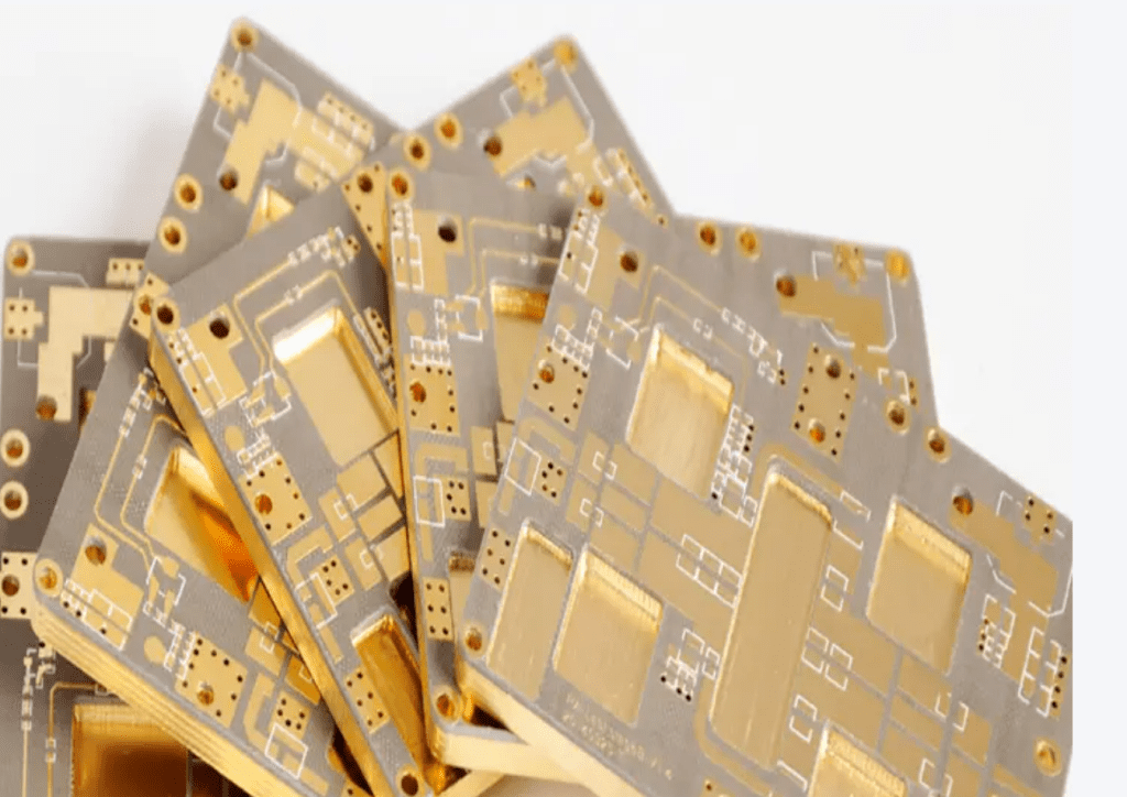
A bare PCB is a fully fabricated printed circuit board that has not yet been populated with electronic components. It consists of a non-conductive substrate material—typically fiberglass-reinforced epoxy (FR-4)—laminated with thin layers of copper that have been etched to form specific conductive pathways. These copper traces serve as the “wiring” that will eventually connect electronic components once they are soldered onto the board. The bare PCB also features a protective solder mask layer (typically green, though other colors are available) that covers the copper traces while leaving the component pads exposed, and a silkscreen layer that provides component identifiers, logos, and other markings for assembly and troubleshooting reference .
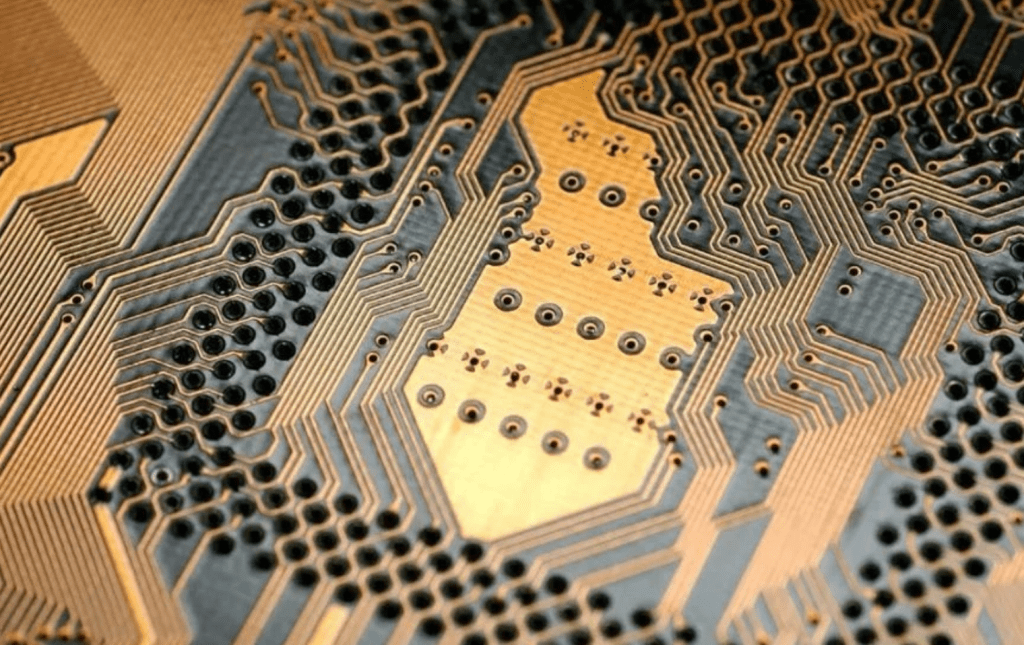
Structurally, a bare PCB contains several essential elements that work together to create a functional interconnection platform. The substrate provides mechanical support and electrical insulation, with FR-4 being the most common material due to its excellent balance of properties including mechanical strength, thermal stability, and electrical insulation. The copper layers form the conductive pathways, with thickness typically measured in ounces per square foot (common weights being 1oz [35μm] and 2oz [70μm]). Vias—plated-through holes—provide electrical connections between different layers in multi-layer boards, with types including through-hole vias (connecting outer layers), blind vias (connecting an outer layer to one or more inner layers), and buried vias (connecting internal layers only). The solder mask protects the copper traces from oxidation and prevents solder bridges during component assembly, while the surface finish (such as HASL, ENIG, or OSP) applied to exposed copper pads ensures solderability and protects against oxidation .
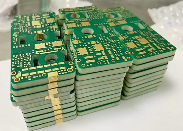
Bare PCBs are categorized based on their construction complexity and application requirements. Single-sided PCBs contain copper traces on only one side of the substrate, representing the simplest and most cost-effective option for basic circuits. Double-sided PCBs feature copper traces on both sides of the substrate, connected by vias, allowing for more complex circuit designs and higher component density. Multi-layer PCBs consist of three or more layers of copper traces separated by insulating layers, enabling high-density interconnections for complex electronic systems. Flexible PCBs use flexible substrate materials like polyimide to allow bending and folding for space-constrained applications, while rigid-flex PCBs combine rigid and flexible sections to provide both structural stability and flexibility where needed .
2 The Significance of Bare PCBs in PCB Manufacturing
In the PCB manufacturing ecosystem, bare PCBs occupy a critical position as the essential intermediary between circuit design conception and functional electronic assembly. The bare PCB serves as the physical manifestation of the circuit schematic, translating abstract electrical connections into precise, reliable physical pathways. This transformation from design to tangible product represents a crucial value-adding step in electronics manufacturing, where the quality of the bare PCB directly determines the performance, reliability, and manufacturability of the final electronic product. Statistical process control data indicates that investments in bare PCB quality yield substantial returns, with each dollar spent on improving bare PCB quality potentially saving up to ten dollars in field failures and warranty claims .
From a technical perspective, bare PCBs enable the implementation of complex circuit designs that would be impractical or impossible with other interconnection methods. The multi-layer construction of modern bare PCBs allows for high-density interconnections supporting complex integrated circuits with pin counts exceeding 1000, while controlled impedance traces maintain signal integrity at multi-gigabit data rates. The materials and construction techniques used in bare PCBs also provide essential thermal management, with standard FR-4 substrates offering thermal conductivity of approximately 0.3 W/m·K, while specialized metal-core and ceramic substrates can provide significantly higher thermal performance for power electronics applications. These technical capabilities make bare PCBs indispensable across the electronics industry, from consumer devices to mission-critical systems in aerospace, medical, and automotive applications .
The bare PCB also plays a crucial role in the manufacturing efficiency and scalability of electronic products. By providing a standardized, reproducible platform for component assembly, bare PCBs enable automated, high-volume manufacturing processes such as surface-mount technology (SMT) assembly, which can place and solder thousands of components per hour with exceptional precision and reliability. This manufacturing efficiency, combined with the ability to test and verify the circuit infrastructure before component assembly, significantly reduces overall manufacturing costs and improves time-to-market for new electronic products. The bare PCB thus serves not only as an electrical interconnection platform but also as a key enabler of modern electronics’ mass production capabilities .
3 What Materials Are Used to Make Bare PCBs?
Bare PCBs are constructed from a carefully selected combination of materials that together provide the necessary electrical, mechanical, and thermal properties required for reliable circuit operation. The substrate, or base material, forms the foundation of the PCB, with FR-4 (fire-retardant epoxy fiberglass) being the most prevalent choice due to its balanced performance characteristics and cost-effectiveness. FR-4 consists of woven fiberglass cloth impregnated with an epoxy resin, offering good mechanical strength (tensile strength of approximately 70-350 MPa), excellent electrical insulation (dielectric strength typically >20 kV/mm), and moderate thermal resistance (glass transition temperature Tg of 130-140°C for standard grades). For applications requiring enhanced thermal performance, high-Tg FR-4 (Tg > 170°C) or polyimide materials are used, while high-frequency applications may employ specialized materials like PTFE or ceramic-filled composites with controlled dielectric constants and lower loss tangents .
The conductive elements of bare PCBs primarily use copper due to its excellent electrical conductivity (5.96×10⁷ S/m), relatively low cost, and good solderability. Copper foil thickness typically ranges from 12μm to 70μm (⅓ oz to 2 oz per square foot), with thinner foils enabling finer feature sizes and thicker foils supporting higher current-carrying capacity. The copper layers are supplemented by various surface finishes that protect exposed copper from oxidation and enhance solderability. Common surface finishes include Hot Air Solder Leveling (HASL), which provides a thick, reliable solderable surface; Electroless Nickel Immersion Gold (ENIG), offering a flat, oxidation-resistant surface ideal for fine-pitch components; and Organic Solderability Preservative (OSP), a thin, environmentally friendly coating that preserves solderability until assembly .
Table: Common Bare PCB Materials and Their Properties
| Material Type | Key Characteristics | Typical Applications | Advantages | Limitations |
|---|---|---|---|---|
| FR-4 | Dielectric constant ~4.5, Tg 130-180°C, cost-effective | Consumer electronics, industrial controls | Balanced properties, wide availability | Moderate high-frequency losses |
| High-Tg FR-4 | Tg > 170°C, enhanced thermal resistance | Lead-free assembly, automotive electronics | Withstands higher temperatures | Higher cost than standard FR-4 |
| Polyimide | Tg > 250°C, excellent flexibility | Flexible circuits, high-temperature applications | Thermal stability, dynamic flexibility | Higher cost, more difficult processing |
| PTFE-based | Low dielectric constant (2.0-2.5), low loss tangent | High-frequency RF/microwave circuits | Superior high-frequency performance | Higher cost, challenging dimensional stability |
| Metal-core | High thermal conductivity (1-4 W/m·K) | Power electronics, LED lighting | Excellent heat dissipation | Electrical isolation challenges |
| Ceramic-filled | Controlled CTE, thermal conductivity | High-reliability applications | Thermal management, stability | Brittle, higher cost |
Additional materials complete the bare PCB structure. The solder mask, typically a liquid photoimageable polymer applied to both sides of the board, serves to protect the copper traces from oxidation, prevent solder bridges during assembly, and provide electrical insulation. Silkscreen, usually epoxy-based ink, adds component designators, test points, and other markings to facilitate assembly and troubleshooting. For multi-layer boards, prepreg (pre-impregnated) materials—typically glass fabric impregnated with partially cured resin—serve as adhesive layers between core materials during the lamination process, flowing to fill gaps and creating a solid, unified structure when heat and pressure are applied. The specific combination of these materials is selected based on the electrical, thermal, mechanical, and cost requirements of each application, with material choices significantly impacting the PCB’s performance, reliability, and manufacturability .
4 Types of Bare Circuit Boards
Bare PCBs are categorized into several distinct types based on their construction methodology, layer count, and material flexibility, with each type offering specific advantages for different applications. The most fundamental classification is based on the number of conductive layers and their arrangement. Single-sided PCBs feature copper traces on only one side of the substrate, representing the simplest and most cost-effective construction suitable for basic circuits with low component density. Double-sided PCBs contain copper layers on both sides of the substrate, connected by plated-through holes (vias), allowing for more complex interconnections and higher component density. Multi-layer PCBs incorporate three or more copper layers separated by insulating dielectric materials, enabling complex, high-density interconnections required for advanced electronic systems such as computers, telecommunications equipment, and sophisticated control systems .
Beyond layer count, bare PCBs are further classified by their mechanical properties and flexibility. Rigid PCBs, the most common type, use solid substrate materials like FR-4 that provide structural stability but cannot be bent or flexed during use. Flexible PCBs employ bendable substrate materials such as polyimide, allowing them to conform to unusual shapes or withstand repeated flexing in applications like wearable electronics, folding smartphones, and moving mechanical assemblies. Rigid-flex PCBs combine rigid and flexible sections in a single structure, providing both stable mounting platforms for components and flexible interconnections between rigid sections, particularly valuable in aerospace, medical, and military applications where reliability, space savings, and three-dimensional packaging are critical requirements .
Specialized bare PCB types address specific application requirements that standard constructions cannot meet. High-frequency PCBs use specialized low-loss dielectric materials with controlled dielectric constants (such as PTFE-based substrates) to maintain signal integrity at microwave and millimeter-wave frequencies. Metal-core PCBs incorporate a metal baseplate (typically aluminum or copper) to provide enhanced thermal management for high-power applications like LED lighting and power converters. High-density interconnect (HDI) PCBs utilize advanced construction techniques including microvias (diameters ≤150μm), fine line widths/spacings (≤75μm), and sequential lamination to achieve higher interconnection density than conventional PCBs, enabling the miniaturization trend in portable electronics and advanced packaging applications. Each PCB type offers distinct advantages and involves specific manufacturing considerations, with selection depending on the electrical, thermal, mechanical, and cost requirements of the target application .
5 How Are Bare Circuit Boards Manufactured?
The manufacturing process for bare PCBs is a complex, multi-step sequence that transforms raw materials into precise, reliable circuit structures. The process begins with the preparation of the substrate material, typically copper-clad laminate sheets that are cut to the required panel size. For multi-layer boards, the inner layers undergo a pattern transfer process where the circuit image is printed onto the copper using a UV-sensitive photoresist. The panels are then exposed to ultraviolet light through a photomask containing the circuit pattern, which hardens the photoresist in the desired circuit areas. The unexposed photoresist is then chemically removed, and the exposed copper is etched away, leaving only the desired circuit pattern protected by the hardened photoresist. After etching, the remaining photoresist is stripped, revealing the precise copper circuit pattern on the inner layers .
For multi-layer boards, the subsequent steps involve layer alignment and lamination. The inner layer cores, prepreg sheets (partially cured epoxy resin with glass fiber reinforcement), and copper foil for outer layers are stacked in precise alignment according to the layer sequence specified in the design. This stack is placed in a lamination press where heat (typically 180-200°C) and pressure (200-300 psi) are applied, causing the prepreg to flow and bond the layers together into a solid panel. After lamination, the panel undergoes drilling operations where holes for through-hole components and vias are created using computer-controlled drilling machines with carbide drill bits. For high-density designs with small features, laser drilling may be employed to create microvias with diameters as small as 50μm. The drilled holes are then plated with copper to establish electrical connections between layers through an electrodes copper deposition process followed by electroplating to build up the required copper thickness .
The outer layers undergo a similar pattern transfer process as the inner layers, after which the board receives its final finishes. A solder mask is applied over the copper traces, typically through screen printing or curtain coating, and then exposed and developed to open holes for component pads and vias. The solder mask is cured in an oven, after which the surface finish (such as ENIG, HASL, or OSP) is applied to protect the exposed copper pads and ensure solderability. Finally, the silkscreen legend is printed using epoxy ink to add component designators, test points, and other markings. Electrical testing, typically using flying probe or fixture-based test systems, verifies circuit continuity and isolation. The individual PCBs are then separated from the production panel by routing or scoring, and a final quality inspection ensures they meet all specifications before shipment .
6 Advantages of Bare PCBs
Bare PCBs offer numerous advantages that have established them as the dominant interconnection technology for electronic systems across all industries. The fundamental advantage lies in their ability to provide reliable, repeatable interconnections for complex electronic circuits in a compact, cost-effective package. The standardized manufacturing processes for bare PCBs enable high-volume production with exceptional consistency and quality, with modern facilities achieving first-pass yields exceeding 98% for standard designs. This manufacturing efficiency translates to lower costs, with complex multi-layer PCBs often costing less than alternative interconnection methods while offering superior performance and reliability. The scalability of PCB manufacturing supports everything from prototype quantities to mass production volumes, making the technology accessible for both development projects and commercial products .
From a technical perspective, bare PCBs provide excellent electrical characteristics that support high-performance electronic systems. Controlled impedance traces enable reliable signal transmission at multi-gigabit data rates, while proper grounding schemes and layer stacking minimize electromagnetic interference. Thermal management is integrated through the substrate material selection, with standard FR-4 providing adequate cooling for many applications, while specialized metal-core and ceramic substrates offer enhanced thermal performance for power electronics. The physical structure of PCBs provides mechanical support and protection for delicate components, with the solder mask and surface finishes safeguarding copper traces from environmental factors such as moisture, contamination, and oxidation. This combination of electrical, thermal, and mechanical properties makes bare PCBs suitable for virtually every electronic application, from consumer devices to extreme environment systems in aerospace and automotive applications .
The design flexibility of bare PCBs represents another significant advantage, allowing engineers to optimize the circuit layout for specific performance, size, and cost targets. Modern design tools support complex routing strategies including high-density interconnects, differential pairs, and controlled impedance traces that can be precisely simulated and optimized before manufacturing. This design capability, combined with the wide range of available materials and constructions, enables bare PCBs to meet diverse application requirements from low-cost consumer products to high-reliability military and aerospace systems. The standardization of PCB design and manufacturing processes also facilitates supply chain efficiency, with numerous qualified manufacturers worldwide capable of producing boards to consistent quality standards, reducing procurement risks and lead times for electronic product developers .
7 Bare Boards vs. Assembled Boards
The distinction between bare boards and assembled boards represents a fundamental division in the PCB hierarchy, with each serving distinct roles in the electronics manufacturing ecosystem. A bare board, as discussed throughout this article, is the unpopulated circuit board containing only the substrate, copper traces, protective layers, and surface finish—essentially the interconnection infrastructure without active or passive components. In contrast, an assembled board (often called PCBA for Printed Circuit Board Assembly) is a bare board that has been populated with electronic components such as resistors, capacitors, integrated circuits, and connectors, which are soldered to the pads and traces to create a functional electronic circuit. The transformation from bare board to assembled board represents the critical transition from passive interconnection structure to active electronic system, where the board gains its intended functionality .
The manufacturing processes for bare boards and assembled boards differ significantly in their complexity, requirements, and objectives. Bare board fabrication focuses on creating precise, reliable conductive pathways on the substrate material, with quality measured primarily in terms of dimensional accuracy, copper integrity, and laminate quality. The process is largely chemical and mechanical, involving etching, plating, and lamination operations. Board assembly, on the other hand, focuses on accurately placing and permanently attaching components to the bare board, with quality measured in terms of placement accuracy, solder joint integrity, and electrical functionality. The assembly process combines mechanical placement operations with thermal processes (reflow soldering, wave soldering) to establish both mechanical and electrical connections between components and the board .
From a testing and validation perspective, bare boards and assembled boards require different approaches and equipment. Bare board testing focuses primarily on continuity (verifying that intended connections exist) and isolation (verifying that unintended connections do not exist), typically using flying probe or bed-of-nails test systems that check for opens and shorts. Assembled board testing is substantially more complex, requiring verification that each component functions correctly and interacts properly with other components in the circuit. This may involve in-circuit testing (measuring individual component values and functionality), functional testing (verifying the board operates as intended in its application), and boundary scan testing (verifying digital logic and interconnections). The substantially higher value of assembled boards (due to the cost of components) makes comprehensive testing more economically justifiable, while the lower value of bare boards necessitates faster, higher-throughput test approaches .
Conclusion
Bare PCBs represent one of the most critical enabling technologies in modern electronics, providing the fundamental platform upon which virtually all electronic systems are built. Their sophisticated combination of materials, manufacturing processes, and design principles enables the complex, reliable interconnections required by today’s electronic devices across all sectors, from consumer products to advanced industrial, automotive, and aerospace systems. The continued evolution of bare PCB technology—driven by trends toward higher density, greater performance, and improved reliability—ensures that these unpopulated boards will remain essential components in the electronics ecosystem for the foreseeable future .
Looking forward, several trends are shaping the development of bare PCB technology. The ongoing miniaturization of electronic devices drives demand for higher density interconnects, with high-density interconnect (HDI) technologies enabling finer features and more complex layer structures. The proliferation of high-speed digital systems and RF applications necessitates improved dielectric materials with controlled properties for signal integrity management. Increasing power densities in electronic systems create requirements for enhanced thermal management solutions, including advanced metal-core and ceramic substrates. Environmental considerations continue to influence material selection and manufacturing processes, with lead-free compatible materials and halogen-free laminates becoming increasingly standard. These developments, combined with advances in design tools and manufacturing capabilities, ensure that bare PCB technology will continue to evolve to meet the demanding requirements of next-generation electronic systems .


0 Comments