
Introduction
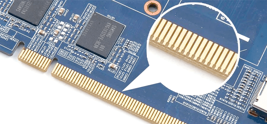
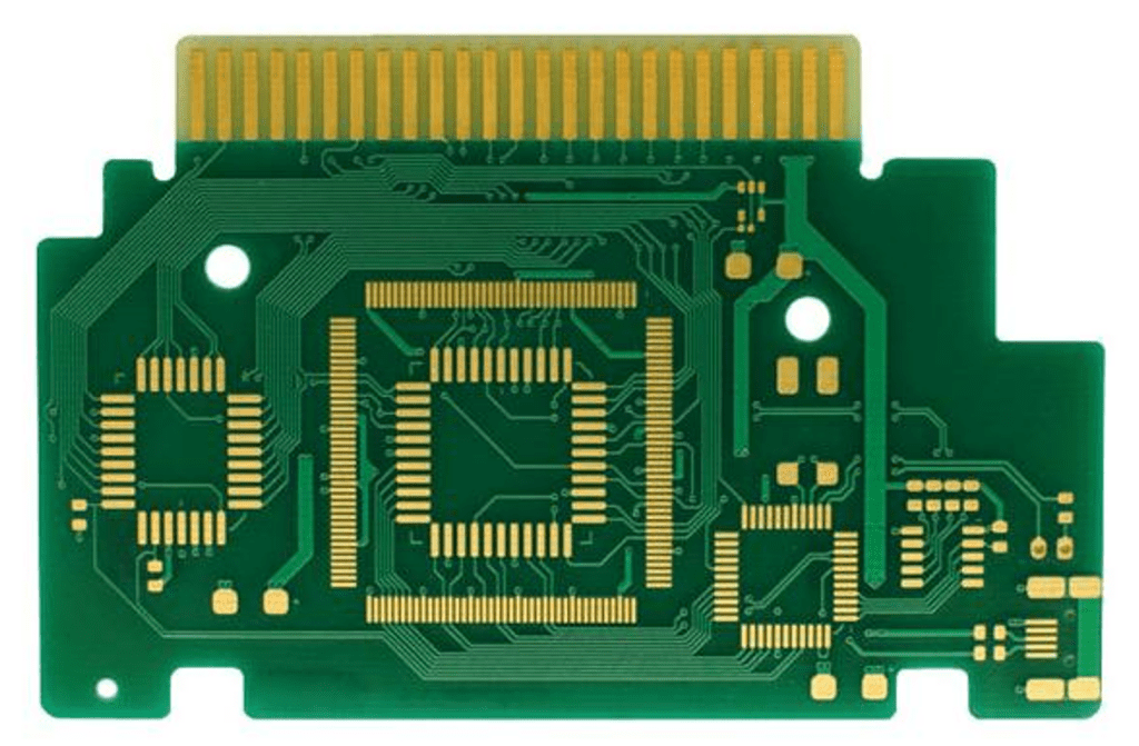
Gold fingers are gold-plated conductive contacts located along the edge of printed circuit boards (PCBs), serving as critical interconnection points for signal transmission and power supply between the PCB and external devices or motherboards. These components, named for their finger-like appearance and gold plating, are particularly prevalent in computer hardware such as memory modules, graphics cards, and various expansion cards, where they plug into corresponding slots (e.g., PCIe, AGP) to establish reliable electrical connections. The primary function of gold fingers is to provide a durable, oxidation-resistant interface that maintains stable electrical performance even after repeated insertion and withdrawal cycles .
The importance of gold finger design in modern electronics cannot be overstated. As an essential element for device upgradability and modular functionality, gold fingers enable the integration of specialized components like sound cards, network cards, and advanced graphics processing units. Industry data indicates that approximately 7% of the world’s gold reserves are utilized in electronic connectors, highlighting their significance in the technology sector. Gold fingers must comply with international standards such as IPC-6010 and IPC-A-600, ensuring reliability across diverse applications from consumer electronics to aerospace systems. With the trend toward miniaturization and higher data rates in 5G communications and IoT devices, precision gold finger design has become increasingly crucial for maintaining signal integrity in high-frequency applications .
1. What are Gold Fingers in PCBs?
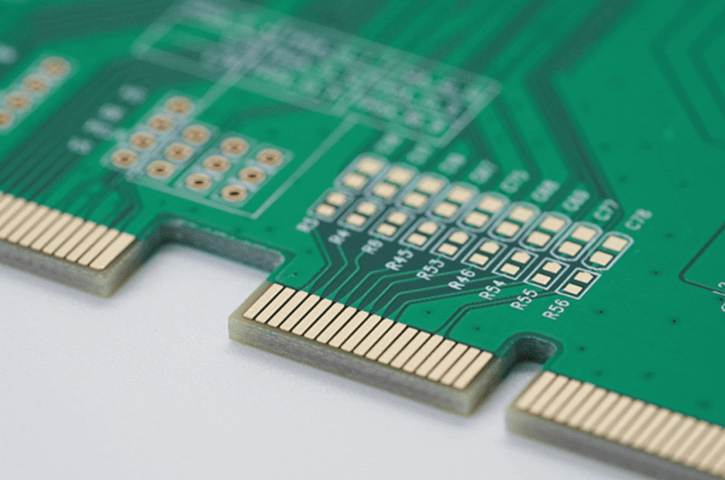
Gold fingers are conducting contact points plated with gold that are positioned along the edges of printed circuit boards to facilitate electrical connections with other circuit boards or electronic devices. Structurally, they consist of three primary layers: a base copper layer (typically 35-70μm thick) that provides the primary conductive path, a nickel barrier layer (3-5μm thick) that prevents copper-gold diffusion, and an outer gold layer (0.8-50μm thick) that ensures excellent conductivity and corrosion resistance. These contacts operate on a pressure contact mechanism, where insertion into a connector creates firm contact with spring-loaded contacts, establishing reliable electrical pathways for signal transmission and power delivery .
From a technical perspective, gold fingers can be categorized into several types based on their configuration and application. Standard gold fingers feature uniformly sized contacts, while staggered or differentiated gold fingers have varying lengths to establish connections in a specific sequence—particularly useful for hot-swappable applications where power connections must engage before signal lines. Segmentated gold fingers appear disjointed and are designed for harsh environments where resistance to moisture ingress is critical. In terms of layout, they can be single-sided (contacts on one side of the PCB) or double-sided (contacts on both sides), with the latter being common in high-speed interfaces like PCIe slots .
The manufacturing process for gold fingers involves sophisticated plating techniques, primarily electroplating hard gold. The process begins with copper foil patterning on the PCB substrate, followed by nickel plating (3-5μm) as a diffusion barrier, and finally gold plating (0.8-3.0μm for commercial applications). The gold layer typically consists of a gold-cobalt alloy (with 5-10% cobalt) that enhances hardness to 150-200 HV, significantly improving wear resistance. This complex process requires precise control of parameters such as current density, solution temperature, and pH levels to ensure uniform thickness and optimal performance .
Table: Gold Finger Types and Characteristics
| Type | Structural Features | Primary Applications | Advantages |
|---|---|---|---|
| Standard Gold Fingers | Uniform length, even spacing | Memory modules, standard expansion cards | Simple manufacturing, cost-effective |
| Staggered/Differentiated Fingers | Contacts of varying lengths | Hot-swappable devices, power management | Sequential power-up, enhanced safety |
| Segmentated Gold Fingers | Disjointed appearing segments | Rugged environments, hybrid technology devices | Moisture resistance, enhanced durability |
| Interdigitated Gold Fingers | Alternating arrangement | High-density connections | Increased contact density, space-saving |
2. Why Use Gold in PCB Gold Fingers?
Gold is the preferred material for PCB contact surfaces due to its exceptional electrical and mechanical properties that make it ideally suited for reliable connection interfaces. Electrically, gold offers excellent conductivity with a resistivity of approximately 2.44 μΩ·cm, which is crucial for maintaining signal integrity, especially in high-frequency applications. Unlike other highly conductive metals like silver and copper, gold does not form oxide layers on its surface, ensuring stable contact resistance over time—a critical factor for low-voltage applications where even thin oxide films could cause connection failures. This combination of properties makes gold particularly valuable in applications where consistent electrical performance is essential, such as in data center equipment, communication infrastructure, and high-reliability automotive systems .
From a mechanical perspective, gold’s moderate hardness, when alloyed with elements like cobalt or nickel, provides an optimal balance between wear resistance and insertion durability. Hard gold plating, with a typical hardness of 150-200 HV, can withstand up to 1,000 insertion-removal cycles without significant degradation, far exceeding the lifespan of alternative coatings. This durability is particularly important for frequently connected and disconnected components, such as test equipment, modular systems, and field-replaceable units. The inherent ductility of gold allows it to accommodate minor misalignments and connector stresses without cracking, maintaining electrical continuity under mechanical stress .
When compared to other surface finishes, gold demonstrates clear advantages despite its higher cost. Silver, while slightly more conductive, is prone to sulfidation which forms non-conductive silver sulfide films. Tin, though inexpensive, oxidizes readily and exhibits poor wear resistance, making it suitable only for low-cost, low-reliability applications. The lifecycle cost of gold finishes often proves more economical despite higher initial expense, as they require less maintenance and provide longer service life without degradation. For high-reliability applications in automotive, aerospace, and medical electronics, the superior performance of gold justifies its premium cost .
Table: Performance Comparison of Contact Surface Materials
| Material | Conductivity | Corrosion Resistance | Hardness | Typical Applications | Relative Cost |
|---|---|---|---|---|---|
| Gold | Excellent | Exceptional | Moderate (when alloyed) | High-reliability connectors | High |
| Silver | Best | Poor (prone to sulfidation) | Relatively soft | High-frequency circuits (as coating) | Medium-High |
| Copper | Very Good | Poor (easily oxidized) | Moderate | General circuitry | Low |
| Tin | Good | Moderate | Soft | Low-cost connectors | Lowest |
The thickness of the gold layer is carefully selected based on application requirements. For high-durability applications such as test interfaces or frequently swapped cards, electroplated hard gold thickness typically ranges from 1.3-3.0μm. For consumer electronics with limited mating cycles, a thickness of 0.8-1.3μm may suffice. The gold layer is typically deposited over a 2-5μm nickel barrier layer that prevents copper diffusion and provides a firm foundation for the gold coating. This layered structure ensures both mechanical durability and long-term electrical stability, making it suitable for various operating environments .
3. PCB Gold Finger Design and Specifications
The design of PCB gold fingers involves meticulous attention to geometric parameters, material selection, and layout considerations to ensure reliable operation throughout the product lifecycle. Geometric parameters form the foundation of gold finger design, with width typically ranging between 1.0-2.5mm and spacing not less than 0.5mm to ensure adequate insulation strength and signal integrity. The length design must consider insertion sequencing, particularly in staggered configurations where longer fingers (typically extended by 1.5-2.0mm) ensure power connections establish before signal lines—a crucial safety feature for hot-swappable applications. These dimensional considerations directly impact the electrical performance and mechanical reliability of the connection interface .
Beveling design represents a critical mechanical aspect of gold fingers. The bevel angle typically ranges from 30-45 degrees, with the depth proportional to board thickness. For a standard 1.6mm board thickness, the safe distance from the board edge is approximately 0.8mm to prevent copper exposure during the beveling process. This angled edge facilitates easier insertion, reduces connector wear, and guides the PCB properly into its slot. Improper beveling can lead to difficult insertion, damaged contacts, and premature connector failure. The beveling process must be precisely controlled to maintain consistent angles across all fingers, ensuring uniform contact pressure and reliable electrical connections .
Solder mask definition is another crucial design element. The gold finger area must be completely free of solder mask, with the opening typically extending 0.25mm (10 mil) beyond the finger pattern. This prevents solder mask residue between fingers, which could dislodge during repeated insertions and contaminate the connector. Additionally, vias within 2mm of gold fingers should have solder mask dammed or plugged to prevent wicking of plating solutions or flux during assembly. Proper solder mask design ensures clean contact surfaces and prevents intermittent connections caused by contamination .
Table: Gold Finger Design Specifications Based on Board Thickness
| Board Thickness (mm) | Minimum Board Edge Distance (mm) | Recommended Bevel Angle (°) | Copper Relief Area Width (mm) |
|---|---|---|---|
| 0.8 | 0.4 | 30-45 | ≥3.0 |
| 1.0 | 0.5 | 30-45 | ≥3.0 |
| 1.2 | 0.6 | 30-45 | ≥3.0 |
| 1.6 | 0.8 | 30-45 | ≥3.0 |
| 2.0 | 1.0 | 30-45 | ≥3.0 |
Impedance control is particularly important for high-speed applications. To achieve consistent impedance (typically 90-100Ω differential), the area beneath gold fingers often undergoes copper relief, where all inner layer copper is removed to create a uniform dielectric environment. This practice also reduces impedance discontinuities between the gold finger and transmission lines. For high-speed interfaces like PCIe 5.0, impedance tolerance must be tightly controlled within ±10% to prevent signal reflection and maintain signal integrity at data rates exceeding 32 GT/s .
Panelization design considerations affect manufacturing yield and quality. For small PCBs (under 40×40mm), special panelization approaches are necessary, ensuring gold finger width exceeds 40mm prior to beveling to facilitate processing. Gold fingers should face inward during panelization to simplify the addition of plating buses. V-cut lines must maintain a minimum distance of 5mm from gold finger areas to prevent damage during depanelization. These design-for-manufacturing considerations significantly impact production efficiency and final quality .
4. PCB Gold Finger Plating Process
The plating process for gold fingers is a sophisticated electrochemical operation that demands precise control over numerous parameters to achieve the required durability and electrical characteristics. The electroplating hard gold method represents the primary approach for applications requiring frequent mating cycles. This process involves electrolytic deposition of a gold-cobalt alloy onto the nickel-coated copper fingers, with typical gold thickness ranging from 0.8-3.0μm for commercial applications and up to 50μm for extreme durability requirements. The process begins with thorough cleaning and micro-etching of the copper surface to ensure proper adhesion, followed by nickel plating (3-5μm) which serves as a diffusion barrier. The gold plating bath typically operates at 50-70°C with careful control of current density (10-20 ASF) to ensure uniform deposition across all fingers .
Electroless nickel immersion gold (ENIG) offers an alternative for applications with less demanding wear requirements but higher need for planarity. This autocatalytic process deposits a thinner gold layer (0.05-0.20μm) over a nickel-phosphorus layer, providing excellent surface planarity beneficial for fine-pitch components. While ENIG gold fingers are less durable (withstanding approximately 50 mating cycles), they offer superior planarity for high-density designs and are more cost-effective for applications not requiring frequent mating, such as dedicated internal cards or permanent installations. The process relies on chemical replacement rather than electrical current, resulting in more uniform deposition regardless of finger geometry .
Process control parameters significantly impact plating quality. Solution temperature affects deposition rate—each 10°C increase typically doubles the reaction rate—but excessive temperatures can cause solution decomposition. pH levels must be maintained within a mildly acidic range (5.5-7.5) to ensure optimal deposition quality and rate. Agitation ensures fresh solution contact with the substrate, preventing depletion zones that cause uneven thickness. Modern plating systems employ automated controls to maintain these parameters within narrow windows, ensuring batch-to-batch consistency. Regular analysis of gold concentration and impurity levels is essential for maintaining deposit quality .
Table: Comparison of Gold Plating Methods for Gold Fingers
| Process Parameter | Electroplating Hard Gold | Electroless Nickel Immersion Gold (ENIG) |
|---|---|---|
| Gold Thickness Range | 0.8-3.0μm (up to 50μm possible) | 0.05-0.20μm (up to 0.3μm maximum) |
| Nickel Underlayer Thickness | 3-5μm | 3-5μm |
| Hardness | 150-200 HV (with cobalt) | 100-150 HV |
| Wear Resistance | High (withstands 1000+ mating cycles) | Low (withstands approx. 50 mating cycles) |
| Planarity | Good | Excellent |
| Relative Cost | High | Moderate |
| Typical Applications | Frequently mated connectors, test interfaces | High-density designs, limited-mating applications |
Quality verification of plated gold fingers involves multiple test methods. Thickness measurement using X-ray fluorescence (XRF) ensures compliance with specifications, with measurements taken at multiple points (typically 5-9 per board) to verify uniformity within ±15%. Adhesion testing via tape peel-off (using standards such as IPC-TM-650) confirms adequate bonding between layers. Porosity testing exposes samples to sulfur dioxide or nitric acid vapors to detect base metal exposure through pores. For high-reliability applications, thermal stress testing (exposure to 155°C for 2-8 hours) verifies the plating’s ability to withstand soldering and operational temperatures without blistering or peeling .
Environmental and safety considerations have led to process refinements in recent years. Modern gold plating baths have reduced cyanide content through alternative chemistries, while closed-loop recovery systems minimize drag-out and reduce gold consumption. Wastewater treatment systems effectively recover precious metals while ensuring effluent compliance with environmental regulations. These improvements have made gold finger plating more sustainable while maintaining the high performance required for critical applications .
5. Applications of PCB Gold Fingers
Gold fingers serve as critical interconnection components across diverse electronic applications, with their specific design variations tailored to meet particular operational requirements. In computer hardware, gold fingers are integral to memory modules (DDR4/DDR5), expansion cards (PCIe), and graphics cards, where they facilitate high-speed data transfer between components and the motherboard. Modern DDR5 memory modules employ dense gold finger arrangements with pitches of 0.6-0.8mm, supporting data rates exceeding 4800 MHz. PCIe 5.0 specifications require precise impedance control (85Ω±5%) to maintain signal integrity at speeds up to 32 GT/s. The hot-plug capability enabled by staggered gold fingers allows for system upgrades and maintenance without power-downs, significantly improving system availability in servers and workstations .
Communication equipment extensively utilizes gold fingers in modular architectures such as network switches, routers, and base stations. In 5G infrastructure, radio frequency cards and baseband units interconnect through gold finger interfaces that support hot-swapping for maintenance and upgrades. These applications often employ specialized designs with enhanced corrosion resistance for outdoor installations, and may incorporate mixed-signal contacts that carry both high-speed data and power through the same interface. The reliability of these connections is critical for network uptime, driving requirements for robust plating thickness (typically 1.5-2.0μm) and precise mechanical tolerances to maintain signal integrity in demanding operating environments .
Automotive electronics represent a growing application area for gold fingers, particularly in infotainment systems, advanced driver assistance systems (ADAS), and vehicle control modules. Automotive applications require gold fingers that can withstand temperature cycling from -40°C to 125°C, resist vibration, and maintain reliable connections despite exposure to fuels, oils, and cleaning solvents. The trend toward zonal architectures in vehicle electronics increases the need for reliable interconnects between domain controllers and specialized function modules. Gold fingers in these applications often feature thicker plating (2.0-3.0μm) and specialized designs that maintain stable contact resistance despite thermal expansion differences between materials .
Table: Gold Finger Applications and Technical Requirements
| Application Field | Typical Gold Finger Type | Technical Requirements | Representative Products |
|---|---|---|---|
| Computer Hardware | Staggered fingers, high-density | High-speed signal integrity, 1000+ mating cycles | Memory modules, graphics cards |
| Communication Equipment | Mixed-signal, power+signal combos | Impedance control, corrosion resistance | Network switches, 5G base stations |
| Automotive Electronics | Robust design, thicker plating | Wide temperature range, vibration resistance | ADAS, infotainment systems |
| Industrial Control | Heavy-duty, segmentated | High reliability, extended temperature range | PLCs, motor drives |
| Medical Equipment | High-reliability, precision pitch | Long-term stability, signal integrity | Patient monitors, imaging systems |
Industrial control systems rely on gold fingers for programable logic controllers (PLCs), motor drives, and input/output modules where reliability under harsh conditions is paramount. These applications often employ specialized designs such as segmentated gold fingers that resist moisture ingress in high-humidity environments. The extended temperature requirements (often -40°C to 85°C or wider) and need for resistance to industrial atmospheres containing sulfur compounds drive material selection and plating thickness decisions. Maintenance and upgrade capabilities are essential for minimizing downtime in industrial settings, making the reliability of gold finger connections critically important for overall system availability .
Emerging applications in Internet of Things (IoT) devices, wearable technology, and flexible electronics are driving innovations in gold finger design. Flexible circuits may use thinner gold deposits (0.3-0.8μm) with specialized underlayers that withstand repeated bending. Miniaturization trends continue to reduce pitch sizes, with some high-density applications now approaching 0.3mm pitch. These developments require increasingly precise manufacturing processes and specialized designs that maintain reliability despite more challenging mechanical and electrical requirements .
6. Testing and Inspection
Comprehensive testing and inspection protocols are essential for ensuring gold finger quality and reliability, encompassing dimensional verification, material analysis, and performance validation. Visual inspection serves as the primary quality assessment method, utilizing magnification (10-20x) or automated optical inspection (AOI) systems to identify surface defects such as scratches, dents, contamination, or plating irregularities. According to IPC-A-600 standards, acceptable gold finger surfaces must be smooth and uniform, with no visible defects. The maximum allowable pore density is 5 pores per square centimeter, with individual defect sizes not exceeding 10μm in diameter. Visual inspection also verifies bevel quality, with angle tolerances maintained within ±5° to ensure compatibility with standard connectors. These visual checks represent the first line of defense against quality issues, catching obvious defects before functional testing .
Thickness measurement using X-ray fluorescence (XRF) provides quantitative data on plating conformance. Measurements are typically taken at multiple locations (minimum 5 points per board—four corners and center) to verify uniformity within ±15% of the target thickness. For commercial applications, gold thickness typically ranges from 0.8-1.3μm, while high-reliability applications may require 1.3-3.0μm. The nickel underlayer thickness (typically 3-5μm) is also critical as it prevents copper diffusion and provides a firm foundation for the gold layer. Modern XRF systems can map thickness distribution across entire panels, identifying patterns that may indicate process issues such as non-uniform current distribution or solution flow .
Adhesion assessment employs tape testing per IPC-TM-650 standards to evaluate the bonding between layers. This test involves applying pressure-sensitive tape (such as 3M 600) to the gold finger surface and removing it with a rapid pulling motion. acceptable results show no gold plating transferred to the tape, indicating adequate adhesion. For high-reliability applications, more rigorous thermal stress testing may be conducted, exposing samples to elevated temperatures (155°C for 2-8 hours) to verify that the plating withstands soldering and operational temperatures without blistering or peeling. These tests ensure the gold finger maintains integrity throughout the device’s operational life, particularly important for applications subject to thermal cycling or mechanical stress .
Table: Key Tests for Gold Finger Quality Verification
| Test Method | Parameters Measured | Acceptance Criteria | Reference Standard |
|---|---|---|---|
| Visual Inspection | Surface defects, uniformity | No visible defects, ≤5 pores/cm² | IPC-A-600 |
| Thickness Measurement | Au and Ni layer thickness | Within specification, ±15% uniformity | IPC-4552 |
| Adhesion Test | Interlayer bonding | No plating removal | IPC-TM-650 |
| Solderability Test | Wetting time, force | <2s wetting time, >70% theoretical force | IPC-J-STD-003 |
| Durability Test | Contact resistance after mating cycles | <20% change after specified cycles | IEC-60512 |
Environmental reliability testing simulates real-world conditions to predict long-term performance. Salt spray testing (5% NaCl solution, 24-96 hours exposure) evaluates corrosion resistance, with acceptable specimens showing no corrosion products. Thermal cycling tests (typically -40°C to 125°C, 100+ cycles) verify performance under temperature variations, with contact resistance changes limited to <20% after testing. Mating durability testing involves repeated insertion and removal cycles (up to 1,000 cycles for high-end applications) with continuous monitoring of contact resistance. These accelerated life tests provide confidence in gold finger reliability under expected operating conditions .
Process control testing monitors manufacturing parameters to maintain consistency. Solution composition analysis (gold concentration, impurity levels) ensures bath chemistry remains within specifications. Regular thickness measurements track deposition rates and identify trends requiring adjustment. Statistical process control (SPC) techniques analyze test data to identify variations before they exceed tolerance limits. These proactive measures help maintain consistent quality and reduce the need for corrective actions, improving overall manufacturing efficiency and product reliability .
7. Common Questions and Answers about Gold Finger PCBs
What is the maximum shelf life for gold finger PCBs, and how should they be stored?
The shelf life for gold finger PCBs typically ranges from 6 to 12 months when stored under appropriate conditions—specifically, temperatures of 15-30°C, relative humidity of 40-60%, and protection from corrosive atmospheres. Packaging should include vacuum-sealed anti-static bags with desiccant to minimize exposure to moisture and contaminants. Boards should be isolated from sulfur-containing materials (such as certain types of paper or rubber) that could promote tarnishing. If storage exceeds the recommended period, solderability testing should be conducted before use in production, ideally using a wetting balance test to quantitatively assess performance .
How should discoloration or oxidation on gold fingers be addressed?
Minor oxidation (light yellowing) generally doesn’t affect solderability and can be compensated for with slightly more active flux chemistry. Moderate oxidation (rainbow coloring) suggests the boards should be used within 24 hours, with RA-grade flux recommended. Severe oxidation (dark gray or black) may require cleaning with specialized solutions or mild abrasives, though this approach risks damaging the surface. Prevention through proper storage is preferable—controlling humidity below 60% RH and using nitrogen-purged packaging can extend the oxidation-free period. For critical applications, incoming inspection should include color comparison against standard references to detect early oxidation .
Do gold fingers present tin whisker risks, and how can they be mitigated?
Early gold plating processes carried some whiskering risks, but modern formulations with organic additives and grain refiners have substantially reduced this issue. Additional mitigation strategies include: using matte gold deposits with small grain size (typically <1μm); avoiding mechanical stresses in the coating; and implementing a thermal anneal (1-2 hours at 150°C) to relieve internal stresses. For extreme reliability requirements, such as aerospace applications, a nickel underlayer may be recommended, though this approach transitions the process toward more expensive ENIG finishing. Design measures, including maintaining minimum 0.4mm spacing between conductors, provide additional protection against whisker-induced short circuits .
How do gold fingers affect high-frequency signal integrity?
Gold fingers generally have minimal impact on high-frequency performance up to approximately 10 GHz, as gold is a good conductor with skin effect characteristics similar to copper. For millimeter-wave applications (>30 GHz), surface roughness becomes more critical, and gold fingers’ typically smooth surface (often <0.2μm Ra) provides advantages over rougher finishes. The absence of magnetic materials (unlike ENIG’s nickel layer) makes gold fingers suitable for high-frequency applications where magnetic losses would be problematic. For extreme high-frequency applications, surface roughness should be controlled to <0.1μm Ra, achievable through optimized deposition parameters .
Are gold fingers suitable for high-current applications?
While the thin gold layer itself has limited current-carrying capacity, the primary current conduction occurs through the underlying copper. The gold coating’s melting point of 1064°C provides a safety margin—in overcurrent conditions, the gold will not melt before copper traces are damaged. For high-current designs (>10A), considerations include: ensuring uniform thickness to prevent localized heating; avoiding dependence on plated through-holes as primary current paths; and implementing thermal management strategies. Successful applications include power converters carrying up to 100A, provided the design addresses the fundamental current carrying capacity through appropriate copper weights and thermal management .
Conclusion
Gold finger technology remains an essential interconnection solution in modern electronics, balancing performance, reliability, and cost across diverse applications. As electronic devices continue evolving toward higher speeds, greater densities, and more demanding operating environments, gold finger designs must correspondingly advance to meet these challenges. Current trends include further miniaturization with pitches approaching 0.3mm, increased plating durability to withstand thousands of mating cycles, and enhanced compatibility with high-frequency signals above 50 GHz. The ongoing development of alternative materials and processes, such as selective gold plating and composite coatings, aims to maintain performance while reducing gold content and environmental impact .
The future of gold finger technology will likely focus on addressing the needs of emerging applications while improving sustainability. Nanostructured gold coatings may offer enhanced wear resistance with less material, while advanced design tools incorporating simulation and artificial intelligence can optimize finger geometry for specific mechanical and electrical requirements. The industry continues to develop more environmentally friendly plating processes with reduced cyanide usage and improved recovery systems. As electronics become increasingly pervasive across all aspects of modern life, the humble gold finger will continue playing a vital role in enabling reliable connections between electronic systems .


0 Comments