
Introduction
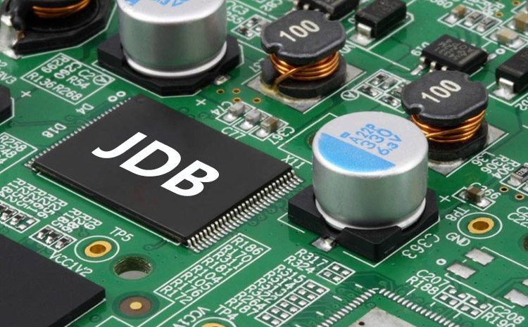
Immersion Tin (ImSn) is a critical surface treatment technology for printed circuit boards (PCBs) that deposits a thin, uniform layer of pure tin onto copper surfaces through a chemical displacement reaction. This process creates a protective coating that prevents copper oxidation while providing excellent solderability. As electronic devices evolve toward higher density and miniaturization, the flat surface profile achieved by immersion tin has become increasingly valuable for fine-pitch components and high-density interconnects.
The significance of immersion tin technology lies in its ability to balance performance, cost, and environmental considerations. Unlike lead-based finishes, immersion tin complies with RoHS directives, supporting the electronics industry’s transition toward environmentally friendly manufacturing. With applications ranging from communication backplanes to automotive electronics, immersion tin has established itself as a reliable surface treatment option, particularly where precise component placement and multiple reflow cycles are required. The technology continues to evolve with improved formulations that address historical limitations such as tin whisker formation and shelf life constraints.
1. What is Immersion Tin PCB?
Immersion Tin PCB refers to a printed circuit board with a copper surface that has been treated through a chemical immersion process to deposit a thin layer of pure tin. This process operates on the principle of galvanic displacement, where copper atoms oxidize and dissolve into solution while tin ions reduce and deposit onto the copper surface. The resulting coating typically ranges from 0.8-1.5μm in thickness and forms a uniform, solderable surface ideal for modern electronic assembly processes.
The fundamental chemical reaction involves the substitution of copper atoms with tin ions from solution, creating a metallurgical bond without requiring external electrical current. This chemical process produces a consistent layer thickness across complex geometries, including high-aspect-ratio through-holes and fine-pitch traces. The tin layer itself consists of pure tin crystals whose size and orientation can be optimized through process parameters such as solution temperature, immersion time, and organic additives. Modern immersion tin formulations incorporate specialized additives that promote fine-grained structures, enhancing the coating’s solderability and resistance to environmental degradation.
A critical aspect of immersion tin technology is the formation of a copper-tin intermetallic compound (IMC) at the interface between the tin layer and copper substrate. This IMC layer, primarily composed of Cu₆Sn₅, provides strong adhesion but continues to grow during storage and thermal processing. The growth rate of this IMC layer typically ranges from 0.14-0.17 nm/s at room temperature, meaning that after 30 days of storage, approximately 0.23μm of tin is consumed through IMC formation. This characteristic necessitates careful consideration of storage conditions and time between PCB fabrication and assembly.
Table: Key Characteristics of Immersion Tin Surface Finish
| Parameter | Typical Value/Range | Standard/Measurement | Significance |
|---|---|---|---|
| Thickness Range | 0.8-1.5 μm | X-ray fluorescence (XRF) | Solderability reliability |
| IMC Growth Rate | 0.14-0.17 nm/s (at 25°C) | Cross-section analysis | Determines effective shelf life |
| Surface Flatness | <0.2 μm Ra | Profilometer | Critical for fine-pitch components |
| Tin Purity | >99.5% | EDX analysis | Solder joint reliability |
| Process Temperature | 50-70°C | Thermal control | Affects deposition rate and uniformity |
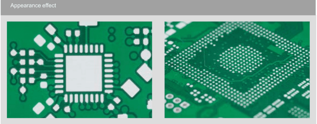
The visual appearance of immersion tin is typically matte gray, distinguishing it from the brighter finish of tin-lead alloys or the yellowish hue of some gold finishes. This appearance results from the microscopic crystal structure of the deposited tin and indicates a chemically active surface suitable for soldering. The finish provides minimal increase to electrical resistance since tin itself is a good conductor with a volume resistivity of approximately 11.5 μΩ·cm.
2. Advantages of Immersion Tin Surface Finish
Immersion tin offers several significant advantages that make it a preferred choice for many PCB applications. The most notable benefit is its exceptional surface flatness, which is crucial for the successful assembly of fine-pitch components. Unlike hot air solder leveling (HASL) which produces uneven surfaces with thickness variations up to 2.5μm, immersion tin provides consistent layer thickness with variations typically within ±0.1μm. This uniformity enables reliable stencil printing for components with pitches below 0.3mm, including modern BGA and QFN packages.
The solderability performance of immersion tin is outstanding, particularly with lead-free solder alloys. Since the coating is pure tin, it exhibits excellent compatibility with all tin-based solders, resulting in high wetting forces and rapid intermetallic formation during reflow. Studies show that immersion tin can achieve wetting spread ratios exceeding 90%, comparable to more expensive finishes like ENIG. The finish withstands multiple reflow cycles—typically 3-5 cycles—without significant degradation of solderability, making it suitable for complex multi-stage assembly processes.
From an economic perspective, immersion tin provides excellent value, typically costing 30-50% less than gold-based finishes like ENIG or ENEPIG. The chemical consumption is efficient, with high utilization rates of tin from the processing solution. Additionally, the relatively simple process equipment required for immersion tin translates to lower capital investment and operational costs compared to more complex metallization processes.
Environmental compatibility represents another significant advantage. As a lead-free finish, immersion tin fully complies with RoHS directives and other environmental regulations. The process chemicals, while requiring careful control, are generally less hazardous than those used in some alternative finishes. Waste treatment is relatively straightforward, contributing to a smaller environmental footprint compared to finishes containing heavy metals or complex chemical complexes.
The process compatibility of immersion tin with various PCB materials and designs is particularly valuable. It performs well with standard FR-4 substrates as well as high-temperature and high-frequency materials. The finish is suitable for both rigid and flexible PCBs, and its uniform deposition characteristics make it effective for complex geometries including high-aspect-ratio through-holes. For press-fit applications, immersion tin provides sufficient lubricity and deformation characteristics to support reliable interconnection.
3. Step-by-Step Manufacturing Workflow
The immersion tin manufacturing process begins with thorough pretreatment of the PCB. This critical phase ensures the copper surface is properly prepared to receive the tin coating. The process starts with acidic cleaning to remove oxides and contaminants, followed by micro-etching to remove approximately 0.5-1.0μm of copper, revealing a fresh, active surface. The micro-etching step, typically using persulfate or sulfuric acid-hydrogen peroxide systems, must be carefully controlled to achieve uniform roughness without over-etching fine traces. After etching, the boards undergo thorough rinsing with deionized water to prevent contamination transfer to the immersion tin bath.
The core immersion tin deposition process occurs in temperature-controlled tanks maintained at 50-70°C. PCBs are immersed in the tin solution for 4-8 minutes, during which the chemical displacement reaction deposits the tin layer. The tin ion concentration in the solution typically ranges from 15-25 g/L, with pH maintained in the mildly acidic range of 5.5-7.5. Solution agitation is necessary to ensure uniform ion distribution across the PCB surface, particularly in dense areas with limited solution flow. Modern immersion tin solutions contain organic additive systems that include complexing agents, stabilizers, and grain refiners to control deposition rate and crystal structure.
Post-treatment and quality verification complete the process. After deposition, boards are rinsed with deionized water to remove residual chemicals, followed by drying using forced air or centrifugation. Thickness measurements are taken at multiple locations (typically 5-9 points per board) using X-ray fluorescence to ensure uniformity within specifications. Additional testing may include solderability evaluation, adhesion tests using tape methods, and accelerated aging to predict shelf life. For high-reliability applications, cross-section analysis may be performed to examine the IMC layer structure and thickness.
Table: Key Process Parameters in Immersion Tin Manufacturing
| Process Parameter | Control Range | Measurement Method | Impact of Deviation |
|---|---|---|---|
| Solution Temperature | 50-70°C | Temperature sensor | Low: slow deposition; High: solution decomposition |
| Immersion Time | 4-8 minutes | Timer | Short: insufficient thickness; Long: rough surface |
| Tin Ion Concentration | 15-25 g/L | Atomic absorption spectroscopy | Low: incomplete coverage; High: coarse crystallization |
| pH Level | 5.5-7.5 | pH meter | Low: rapid deposition; High: stalled deposition |
| Solution Agitation | Continuous, uniform | Flow indicators | Uneven deposition without proper agitation |
Throughout the process, cleanroom conditions are maintained to prevent particulate contamination that could create defects. Chemical parameters are monitored and adjusted regularly to maintain bath stability and consistency. For high-reliability products, statistical process control charts track key parameters, with corrective actions triggered when trends approach control limits. The entire process is designed to be repeatable and scalable from prototype to high-volume production.
4. Comparative Analysis with Other Surface Finishes
When evaluated against alternative surface finishes, immersion tin occupies a distinct position in the performance-cost spectrum. Compared to Hot Air Solder Leveling (HASL), immersion tin provides superior surface flatness, which is critical for fine-pitch components. While HASL typically produces surfaces with topography variations of 2-5μm, immersion tin maintains consistency within 0.2μm, enabling more reliable solder joint formation for components with pitches below 0.4mm. However, HASL offers better durability for multiple rework cycles and generally has longer shelf life—up to 12 months versus typically 6 months for immersion tin.
Versus Electroless Nickel Immersion Gold (ENIG), immersion tin is significantly more cost-effective but offers different performance characteristics. ENIG provides excellent oxidation resistance and shelf life (up to 12 months), but at a premium cost of 30-50% or more compared to immersion tin. The nickel layer in ENIG serves as an effective diffusion barrier, maintaining stable solderability over time, while immersion tin continues to form copper-tin intermetallics during storage. For high-frequency applications, immersion tin typically provides better signal integrity than ENIG, as it lacks the magnetic nickel layer that can cause signal loss at high frequencies.
Organic Solderability Preservatives (OSP) represent another alternative, with immersion tin offering advantages in terms of shelf life and visual inspectability. OSP coatings are typically limited to 3-6 months shelf life, while properly processed immersion tin can maintain solderability for 6-12 months. The visible tin layer allows for straightforward visual inspection, whereas OSP coatings are transparent, making defects more difficult to detect. However, OSP is generally lower in cost and provides excellent surface flatness comparable to immersion tin.
Table: Performance Comparison of Common PCB Surface Finishes
| Characteristic | Immersion Tin | HASL | ENIG | OSP |
|---|---|---|---|---|
| Surface Flatness | Excellent | Poor | Excellent | Excellent |
| Solderability | Excellent | Good | Good | Good |
| Shelf Life | 6-12 months | 12 months | 12 months | 3-6 months |
| Cost | Medium | Low | High | Low |
| Fine-Pitch Capability | Excellent (<0.3mm) | Limited (>0.5mm) | Excellent (<0.3mm) | Excellent (<0.3mm) |
| Rework Cycles | 3-5 | 5+ | 2-3 | 1-2 |
Immersion silver offers similar flatness advantages to immersion tin, with comparable cost structure. The key differences emerge in specific application requirements: silver provides better high-frequency performance due to lower surface losses, while tin is generally less susceptible to tarnishing in sulfur-containing environments. For press-fit applications, immersion tin often provides better performance due to its lubricating properties and deformation characteristics.
For high-reliability applications such as automotive or aerospace electronics, immersion tin must be evaluated against more expensive options like ENEPIG. While ENEPIG offers superior wire bonding capability and resistance to corrosive environments, immersion tin provides adequate performance for many applications at a fraction of the cost. The decision between these options ultimately depends on the specific reliability requirements, operating environment, and cost constraints of the end product.
5. Quality Control and Testing Methods
Quality assurance for immersion tin PCBs involves multiple verification methods to ensure consistent performance. Thickness measurement using X-ray fluorescence (XRF) is performed at multiple locations across the panel, with typical specifications requiring uniformity within ±15% of the target thickness. Measurements are taken at a minimum of 5 points—four corners and center—with additional points recommended for large panels or areas with significant density variations. The target thickness typically ranges from 0.8-1.2μm, with minimum values not less than 0.8μm to ensure sufficient tin remains after IMC formation during storage.
Solderability testing according to IPC-J-STD-003 determines the wetting performance of the finish. The wetting balance test measures the time and force with which molten solder spreads across the surface, with acceptable criteria requiring wetting within 2 seconds and achieving at least 70% of the theoretical maximum wetting force. Additional solderability assessment may involve solder dip tests or spread tests using standardized solder alloys. For automotive and other high-reliability applications, testing after accelerated aging (typically 8-16 hours at 85°C/85%RH) verifies maintained solderability after simulated storage.
The tin whisker growth risk assessment involves accelerated testing under temperature cycling (-55°C to 85°C for 100 cycles) or elevated temperature/humidity conditions (60°C/93%RH for 1000 hours). After testing, microscopic examination checks for whisker formation, with acceptable limits typically requiring whiskers shorter than 50μm with no bridging between conductors. The test vehicles include specific patterns designed to promote whisker growth, such as traces with different widths and spacings. Modern immersion tin processes with organic additives typically show significantly reduced whisker formation compared to earlier formulations.
Intermetallic compound analysis through cross-sectioning and microscopic examination determines the thickness and morphology of the copper-tin IMC layer. Scanning electron microscopy with energy-dispersive X-ray spectroscopy (SEM-EDS) identifies the composition and thickness of the IMC, which should ideally be 0.1-0.5μm initially. After thermal aging (typically 3 reflow cycles at 240-260°C), the IMC thickness should not exceed 1.0μm to maintain solder joint reliability. Additionally, solder ball shear or pull testing evaluates the interface strength, with acceptable failure modes being cohesive within the solder rather than at the interface.
Table: Key Quality Tests for Immersion Tin Finishes
| Test Method | Parameters Measured | Acceptance Criteria | Standard Reference |
|---|---|---|---|
| XRF Thickness Measurement | Tin layer thickness | 0.8-1.2μm, ±15% uniformity | IPC-4554 |
| Wetting Balance Test | Wetting time, force | <2s wetting time, >70% of theoretical force | IPC-J-STD-003 |
| Solder Dip Test | Solder spread, dewetting | ≥95% coverage, no dewetting | IPC-TM-650 2.4.14 |
| Tin Whisker Assessment | Whisker density, length | <50μm length, no bridging | JESD22-A121 |
| IMC Thickness Measurement | Cu₆Sn₅ layer thickness | <1.0μm after 3× reflow | IPC-4554 |
Accelerated aging tests simulate long-term storage conditions to predict shelf life. Boards are typically exposed to elevated temperature and humidity (85°C/85%RH) for periods representing 6-12 months of real-world storage. After aging, solderability testing must meet the same criteria as freshly processed boards. Additionally, visual inspection checks for discoloration or oxidation, with any noticeable darkening requiring further analysis to determine if performance is affected.
6. Industry Applications and Case Studies
Immersion tin finds diverse applications across multiple electronics sectors, with particular strength in communication infrastructure equipment. Backplanes and server boards benefit from immersion tin’s flat surface profile, which supports high-density interconnects with signal speeds exceeding 10 Gbps. A leading telecommunications manufacturer reported achieving 98.5% first-pass yield on 20-layer server boards using immersion tin, citing its compatibility with complex press-fit connectors and stability through multiple reflow cycles. The finish’s consistent thickness ensures reliable impedance control critical for high-speed signals.
The automotive electronics sector increasingly adopts immersion tin for engine control units (ECUs), infotainment systems, and advanced driver assistance systems (ADAS). One European automotive supplier documented successful implementation in transmission control modules that withstood 3000 temperature cycles from -40°C to 125°C without solder joint failures. The finish’s compatibility with lead-free soldering processes aligns with automotive industry requirements, while its cost-effectiveness supports the high-volume production typical in this sector. The lubricating properties of tin also facilitate reliable press-fit connections for automotive connectors.
Industrial control systems represent another significant application area, where immersion tin provides reliable performance in harsh operating environments. Programmable logic controllers (PLCs) and motor drives utilizing immersion tin-finished PCBs have demonstrated mean time between failures (MTBF) exceeding 50,000 hours in field studies. The finish resists industrial atmospheres containing moderate levels of sulfur-containing compounds, outperforming silver finishes in these environments. For industrial applications requiring frequent firmware updates or module replacements, immersion tin supports multiple rework cycles without significant degradation.
In the consumer electronics sector, immersion tin balances cost and performance for products including smart televisions, home appliances, and computing equipment. A major consumer electronics manufacturer achieved a 15% cost reduction by transitioning from ENIG to immersion tin for motherboard production without compromising reliability metrics. The finish’s compatibility with advanced packaging technologies, including 0.3mm pitch BGA and micro-BGA components, supports the ongoing trend toward miniaturization in consumer products.
Emerging applications in medical electronics and renewable energy systems are leveraging immersion tin’s reliability and environmental compatibility. Portable medical diagnostic devices benefit from the finish’s consistent performance after sterilization cycles, while solar inverter manufacturers value its stability in outdoor environments. One solar inverter manufacturer reported a 30% improvement in temperature cycling performance compared to OSP finishes when using immersion tin for power conversion boards operating at temperatures up to 105°C.
7. Frequently Asked Questions about Immersion Tin PCBs
What is the maximum shelf life for immersion tin PCBs, and how should they be stored?
The shelf life for immersion tin PCBs typically ranges from 6 to 12 months when stored under proper conditions—specifically, temperatures of 15-30°C, relative humidity of 40-60%, and protection from corrosive atmospheres. Packaging should include vacuum-sealed anti-static bags with desiccant to minimize exposure to moisture and contaminants. Boards should be isolated from sulfur-containing materials (such as certain types of paper or rubber) that could promote tarnishing. If storage exceeds the recommended period, solderability testing should be conducted before use in production, ideally using a wetting balance test to quantitatively assess performance.
How should discoloration or oxidation on the immersion tin surface be addressed?
Minor oxidation (light yellowing) generally doesn’t affect solderability and can be compensated for with slightly more active flux chemistry. Moderate oxidation (rainbow coloring) suggests the boards should be used within 24 hours, with RA-grade flux recommended. Severe oxidation (dark gray or black) may require cleaning with specialized solutions or mild abrasives, though this approach risks damaging the surface. Prevention through proper storage is preferable—controlling humidity below 60% RH and using nitrogen-purged packaging can extend the oxidation-free period. For critical applications, incoming inspection should include color comparison against standard references to detect early oxidation.
Does immersion tin present tin whisker risks, and how can they be mitigated?
Early immersion tin processes carried significant tin whisker risks, but modern formulations with organic additives and grain refiners have substantially reduced this issue. Additional mitigation strategies include: using matte tin deposits with small grain size (typically <1μm); avoiding mechanical stresses in the coating; and implementing a thermal anneal (1-2 hours at 150°C) to relieve internal stresses. For extreme reliability requirements, such as aerospace applications, a nickel underlayer may be recommended, though this approach transitions the process toward more expensive ENIG finishing. Design measures, including maintaining minimum 0.4mm spacing between conductors, provide additional protection against whisker-induced short circuits.
How does immersion tin affect high-frequency signal integrity?
Immersion tin generally has minimal impact on high-frequency performance up to approximately 10 GHz, as tin is a good conductor with skin effect characteristics similar to copper. For millimeter-wave applications (>30 GHz), the surface roughness becomes more critical, and immersion tin’s typically smooth surface (often <0.2μm Ra) provides advantages over rougher finishes. The absence of magnetic materials (unlike ENIG’s nickel layer) makes immersion tin suitable for high-frequency applications where magnetic losses would be problematic. For extreme high-frequency applications, surface roughness should be controlled to <0.1μm Ra, achievable through optimized deposition parameters.
Is immersion tin suitable for high-current applications?
While the thin tin layer itself has limited current-carrying capacity, the primary current conduction occurs through the underlying copper. The tin coating’s melting point of 232°C provides a safety margin—in overcurrent conditions, the tin may melt before copper traces are damaged, potentially acting as a crude fuse. For high-current designs (>10A), considerations include: ensuring uniform thickness to prevent localized heating; avoiding dependence on plated through-holes as primary current paths; and implementing thermal management strategies. Successful applications include power converters carrying up to 100A, provided the design addresses the fundamental current carrying capacity through appropriate copper weights and thermal management.
Conclusion
Immersion tin surface finish represents a balanced solution in the PCB finishing landscape, offering an optimal combination of surface flatness, solderability, and cost-effectiveness. As electronic devices continue toward higher component densities and more complex architectures, the importance of uniform, reliable surface finishes will only increase. The technology has evolved significantly from earlier versions prone to whiskering and limited shelf life, with modern formulations addressing these historical limitations through advanced chemistry and process control.
The future of immersion tin technology points toward continued refinement of organic additives to further suppress whisker formation, enhanced thermal stability for multiple reflow cycles, and compatibility with emerging substrate materials. The drive toward sustainability may also bring developments in recycling and recovery of tin from processing solutions, reducing environmental impact. As a RoHS-compliant finish with proven reliability across diverse applications, immersion tin is well-positioned to maintain its important role in electronic manufacturing.
Selecting immersion tin represents a strategic decision balancing performance requirements with economic realities. For applications where fine-pitch components, complex geometries, and cost sensitivity converge, immersion tin offers a technically sound solution validated through extensive industry experience. By understanding its characteristics, limitations, and optimal application parameters, designers can leverage this finish to produce reliable, high-performance electronic products.


0 Comments