
Introduction
In the realm of modern technology, the world is expanding at an unprecedented pace, with advancements directly influencing our daily activities. Today, numerous sophisticated devices are in use—something unimaginable just a few years ago. Supported by these technological innovations, we continue to enhance our quality of life.
From smartphones and speakers to automobiles, nearly every device incorporates electronic components. At the heart of these electronics lies the PCBA circuit board, enabling devices to function as intended. Electronic engineering serves as the core of these systems, with the PCBA circuit board acting as the central nervous system.
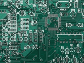
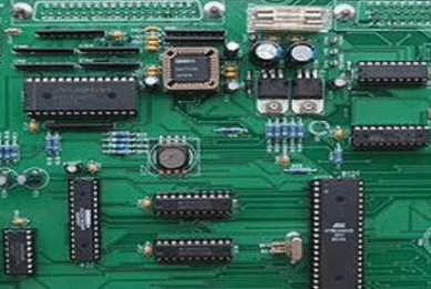
When most people encounter a PCBA circuit board, they can quickly identify it—typically a green board featuring conductive traces and copper pads, found at the center of disassembled electronic devices. These boards are constructed from materials such as fiberglass, copper traces, and various metal parts, interconnected with epoxy and insulated by a solder mask. This solder mask is responsible for their distinctive green color.
A PCBA circuit board refers to a printed circuit board (PCB) populated with electronic components, while the term PCBA (Printed Circuit Board Assembly) denotes the manufacturing process. So, how exactly are these electronic devices produced? The PCB assembly process is relatively straightforward, involving a combination of automated and manual steps. Below, we break down each stage of the PCBA process to provide a comprehensive understanding from start to finish. Let’s dive in.
What is PCB Assembly?
Simply put, PCBA refers to a printed circuit board (PCB) that has been fully populated with electronic components—such as chips, resistors, capacitors, and connectors—through mounting and soldering processes. It is the finished, functional product obtained after a series of assembly procedures, capable of performing specific electrical functions.
Various assembly techniques are employed during manufacturing to produce the final product. PCB assembly is one such critical process. When developing electronic products, manufacturers must consider numerous factors, with one of the most crucial being how to integrate components into a functional unit that operates as designed. Printed Circuit Board Assembly (PCBA) is a key technique in this regard, requiring meticulous preparation before deployment.
In essence, PCB assembly involves placing all necessary elements together and constructing a functional device using various electronic components. It entails taking a newly fabricated circuit board, adding components and resistors, and ensuring it performs according to specifications. Multiple methods are available for creating PCB assemblies, including pick-and-place, reflow soldering, and wave soldering.
It is important to note that circuit board assembly differs from PCB manufacturing. PCB prototyping and PCB design are techniques used to produce the bare printed circuit board. Before being deployed in any electronic device, a PCB must have active and passive electronic components soldered onto it. The type of circuit board, the variety of electronic components, and the intended function of the board all influence how these components are assembled.
Understanding PCBs: From Basic Layers to Different Types
The substrate, composed of multiple layers, forms the most fundamental component of a PCB and is where the assembly process always begins. Each layer plays a vital role in the functionality of the finished PCB. Below, we examine several alternating outer layers and their functions.
Substrate
This serves as the base of the PCB—all other components are mounted onto it. It provides the PCB with rigidity and structural stability.
Copper Layer
A thin layer of conductive copper foil is applied to one or both sides of the PCB, depending on whether it is single-sided or double-sided. This is where the copper trace layer resides.
Solder Mask
This layer is applied to the top and bottom of the PCB, giving it its characteristic green hue. It creates non-conductive areas on the PCB, isolating copper traces from one another to prevent short circuits. Additionally, it prevents solder from adhering to unintended components, ensuring that solder only contacts designated pads and holes.
The use of a solder mask during the PCBA circuit board assembly process is essential for preventing short circuits and unintended soldering.
Silkscreen
The final layer on the PCB is the white silkscreen. This layer adds labels, characters, and symbols to the board, clarifying the purpose of each component.
On the other hand, PCBs can be categorized based on substrate material:
Rigid PCB
Rigid PCBs are solid and inflexible circuit boards. They cannot be bent or twisted and are typically made from rigid plastic substrates that are thicker than standard PCBs. Most PCBs encountered in various devices fall into this category. These boards come in various thicknesses and are known for their strength and durability. The primary material used is fiberglass, commonly referred to as “FR4” (Flame Retardant 4). FR-4 material offers advantages for many industrial electronic applications due to its self-extinguishing properties. Copper-clad laminates, often called copper foil laminates, are layered on both sides of FR-4. While epoxy and phenolic resins are less expensive than FR4, they result in less durable PCBs.
- FR-4 provides:
- High dielectric strength for electrical insulation
- High strength-to-weight ratio
- Lightweight
- Relative heat resistance, ensuring reliable performance under most external conditions
Flexible PCB
Compared to their rigid counterparts, flexible printed circuit boards offer greater adaptability. Flexible PCBs are created by drawing conductive paths onto a dielectric substrate. Each board consists of flexible laminates made from special materials to ensure the final product’s flexibility.
Flexible PCBs offer several advantages over traditional rigid PCBs: they can be made smaller since they do not need to support their own weight; they can be used in spaces where traditional boards are unsuitable; and they can be fabricated from plastic instead of metal, making them more cost-effective and easier to produce.
Types of PCBA Mounting Technologies
Surface Mount Technology (SMT)
Although it has been around for some time, the surface mount technology (SMT) market continues to thrive. SMT involves mounting electronic components onto a PCB, which can vary in size and form depending on the project or product. A range of equipment—such as pick-and-place machines, ovens, and reflow soldering systems—is used in PCB surface mount assembly. Together, these components form a fully functional circuit board capable of performing the specific tasks required by the product or gadget.
SMT is suitable for small components and integrated circuits (ICs). Since the surface mount assembly process can be challenging and time-consuming for manual operation, it is typically performed by automated pick-and-place robots.
Through-Hole Technology (THT)
THT is effectively used for components that require leads or wires to be inserted into holes on the board. The additional lead components must be soldered on the opposite side of the circuit board. This method is used to create PCB assemblies that include larger parts such as capacitors and coils. THT component assembly is generally performed through manual soldering and is relatively straightforward.
Understanding the PCB Assembly (PCBA) Process
Before commencing the actual PCB assembly process, several preliminary tasks must be completed. These help PCB manufacturers verify the functionality of the PCB design, primarily through a Design for Manufacturability (DFM) check. DFM checks identify potential issues before they arise, saving manufacturing costs and minimizing overhead.
The actual PCB assembly process involves the following steps:
Solder Paste Stencil Printing
The first stage of PCB assembly is applying solder paste to the board. This process is similar to screen printing, but instead of a mask, a thin stainless steel stencil is placed over the PCB. Solder paste, a gray substance composed of tiny metal spheres, is made from 96.5% tin, 3% silver, and 0.5% copper. Assemblers use it to apply the paste specifically to areas where components will be mounted on the finished PCB. When heated, this solder paste melts and forms solid joints.
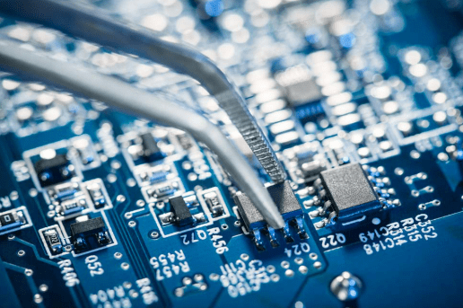
Pick and Place
After solder paste is applied, the PCB assembly process moves to the pick-and-place machine—a robotic device that positions surface-mount devices (SMDs) on the prepared board. SMDs now constitute the majority of non-connector components on PCBs.
Traditionally, this was a manual task requiring assemblers to pick and place components using tweezers. Fortunately, the process is now automated among PCB assemblers, primarily because machines offer greater accuracy and consistency than humans.
Reflow Soldering
Once the solder paste and surface-mount components are in place, they must be secured. This means the solder paste must solidify to attach the components to the board. This is achieved through a process called “reflow soldering.”
The reflow process involves placing the PCB and components on a conveyor belt, which transports them through a large oven heated to approximately 250°C. This temperature causes the solder to melt. The molten solder then bonds the components to the PCB, forming joints. After exposure to high heat, the PCB is cooled. The solder joints are subsequently solidified in a controlled manner by coolers, creating a permanent connection between the SMD components and the PCB.
Quality Control and Inspection
After components are soldered in place via reflow, the PCBA is not yet complete—the finished board must undergo functional inspection. Post-reflow, components may become misaligned due to movement within the PCB fixture tray, leading to short circuits or open connections.
Three common inspection methods are used:
- Manual Inspection: Suitable for boards with THT components and low component density.
- Automated Optical Inspection (AOI): Uses high-power, high-resolution cameras positioned at different angles to examine solder connections from multiple perspectives.
- X-ray Inspection: Allows inspectors to see through layers and visualize underlying structures to identify hidden defects, typically used for more complex or multi-layer PCBs.
Securing and Soldering THT Components
Through-hole components can be found on many PCB boards. These parts are also referred to as plated through-hole (PTH) components. The leads of these components pass through holes in the PCB.
These holes allow the PCB assembly to transmit signals from one side of the board to the other. In this case, solder paste is not effective, as it would flow through the holes without adhering.
In subsequent PCB assembly stages, PTH components require a more complex soldering approach:
- Manual Through-Hole Insertion: A straightforward process involving manual soldering. Typically, an operator inserts a component into a specific PTH at one station. The board is then moved to the next station, where another operator attaches a different component. This process is repeated for each PTH that needs to be populated.
- Wave Soldering: An automated equivalent to manual soldering, but using a completely different procedure. Here, molten solder is applied to the bottom of the board as it passes through a specialized oven on a conveyor. Since wave soldering covers the entire underside of the PCB, it is nearly impossible to use for double-sided boards without damaging delicate electronic components.
Final Inspection and Functional Testing
The PCB is now ready for final inspection and testing. This involves a functional test where the PCB is powered with electrical signals at designated pins, and outputs are checked at specified test points or output connectors. This test requires standard laboratory equipment, including oscilloscopes, digital multimeters, and function generators.
Final Cleaning, Finishing, and Shipping
This is the last step in the PCB assembly process. After the PCB has been inspected and deemed in good overall condition, any remaining flux residue, along with fingerprints and oil stains, must be removed. All forms of contamination can be eliminated using a high-pressure washer made of stainless steel and deionized water. After cleaning, the PCB is dried using compressed air. The finished PCB is now ready for packaging and shipping.
Conclusion
It can be said that the PCBA process serves as the bridge that transforms abstract circuit designs into tangible, functional products. It is not only a concentrated reflection of smart manufacturing and precision engineering but also a cornerstone of modern electronic civilization. Every powerful smart device we hold derives its functionality from this intricate and sophisticated assembly art—quietly supporting the vigorous operation of the entire digital world.
By choosing Thindry as your PCBA circuit board partner, you are opting to collaborate with a company dedicated to delivering optimal results. Our PCB assembly services adhere to the strictest quality standards. Whether for double-sided or single-sided PCBs, SMT, through-hole, or mixed-assembly projects, we have the expertise to handle them all.
Thindry consistently evaluates customer needs to provide high-quality printed circuit board assemblies. Contact us today, and let us help you navigate the PCB assembly process smoothly while saving time and costs!


0 Comments