
Introduction
Soldering on PCB is a foundational process in electronics manufacturing and assembly, directly determining the performance, reliability, and longevity of electronic products. As the core method for establishing electrical and mechanical connections between components and circuit boards, soldering encompasses a range of techniques—from automated processes like reflow and wave soldering to manual methods used in prototyping and repair. This article provides a systematic overview of soldering principles, key methodologies, essential materials, and quality control measures, offering a complete technical framework for engineers, technicians, and enthusiasts engaged in soldering on PCB.
Fundamentals of Soldering
The essence of soldering lies in forming a metallurgical bond between component leads and PCB pads using molten solder, ensuring both electrical conductivity and mechanical strength. The core mechanism is “wetting,” where liquid solder spreads over metal surfaces to form a continuous intermetallic compound (IMC) layer. Achieving optimal wetting requires three fundamental conditions:
- Clean metal surfaces: Pads and leads must be free from oxides and contaminants.
- Suitable flux: Removes residual oxides, reduces surface tension, and promotes wetting.
- Adequate heat input: Provides the energy required to melt the solder and form the IMC layer.
Primary Soldering Methods
- Manual Soldering
- Applications: Prototyping, low-volume production, rework, and field repair.
- Key Tools: Temperature-controlled soldering iron, flux-cored solder wire.
- Process Focus: Relies heavily on operator skill, including temperature control, timing, and heat management.
- Wave Soldering
- Applications: High-volume through-hole component soldering.
- Process: PCBs are passed over a wave of molten solder to wet the plated through-holes and pads.
- Features: High efficiency and consistency, though it imposes layout and orientation constraints.
- Reflow Soldering
- Applications: Predominant method for surface-mount device (SMD) assembly.
- Process: Solder paste is printed onto pads, components are placed, and the assembly passes through a reflow oven following a precise temperature profile.
- Features: High precision, suitable for micro-components and high-density layouts.
Key Materials and Tools
- Solder: Includes tin-lead (e.g., Sn63/Pb37) and lead-free alloys (e.g., SAC305). Lead-free solders meet environmental regulations but present challenges such as higher melting points.
- Flux: Integrated into solder wire or paste, it removes oxides and prevents re-oxidation. Residue removal may be required for high-reliability applications.
- Solder Paste: A critical material in SMT, whose metal content, particle size, and rheology affect print quality and joint formation.
- Soldering Iron: The core tool for manual soldering, whose temperature stability and tip geometry directly impact results.
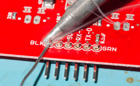
Manual Soldering Standards and Techniques
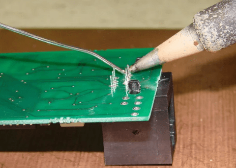
A standardized approach ensures consistent manual soldering quality:
- Preparation: Clean and pre-tin the iron tip; prepare solder wire, flux, and desoldering tools.
- Heat Transfer: Apply the tip to both the lead and pad to reach soldering temperature within 1–3 seconds.
- Solder Feeding: Introduce solder wire from the opposite side of the tip.
- Completion: Withdraw the solder once a concave fillet is formed.
- Tip Removal: Quickly withdraw the iron along the lead axis and allow the joint to cool undisturbed.
- Advanced Techniques
- Pre-Tinning for Alignment: Pre-tin alignment pads to temporarily secure multi-pin connectors.
- Drag Soldering: Use specific tip movements and surface tension to solder and clean dense pin arrays.
- Flux Assistance: Apply additional flux to improve wetting on oxidized surfaces or during drag soldering.
Rework and Desoldering
Rework is integral to soldering on PCB and requires specialized tools:
- Common Tools: Desoldering pumps, wick, hot air rework stations, chip lifters.
- Multi-Pin Component Removal:
- For DIP components: Use a soldering iron with desoldering wick.
- For SMD components: Apply controlled hot air via a nozzle, then lift once solder is molten.
Common Defects and Quality Control
Effective quality control ensures soldering reliability. Common defects include:
- Cold Joints: Result from insufficient heat or contamination, leading to poor electrical connection.
- Solder Bridges: Unintended connections between adjacent pins causing short circuits.
- Disturbed Joints: Characterized by a grainy appearance, caused by movement during solidification.
- Tombstoning: Passive components stand upright due to imbalanced wetting forces.
Inspection methods include visual checks (per IPC-A-610), automated optical inspection (AOI), X-ray imaging (for hidden joints), and electrical testing.
Conclusion
Soldering on PCB is essential throughout the lifecycle of electronic products. From manual operations to fully automated production, the field demands continuous pursuit of precision, reliability, and efficiency. With increasing component density and evolving packaging technologies—such as 3D packaging and system-in-package (SiP)—soldering continues to advance toward finer pitches, lower temperatures, and higher reliability. Ongoing learning and practical experience remain crucial for every professional engaged in soldering on PCB.


0 Comments