
In modern electronics manufacturing, PCB, though small in size, are the “neural network” of electrical and electronic systems. With technological advancements and diversified design requirements, PCB have expanded from traditional rigid boards to include various types and materials. The emergence of flexible PCB has further endowed electronic devices with unprecedented design freedom and reliability. Today, they are widely used in consumer electronics, medical devices, industrial control, smart wearables, robotics, aerospace, and other fields, becoming a vital force driving innovation.
As one of China’s leading PCB manufacturers, Thindry is committed to providing customers with one-stop solutions for flexible PCB and their assembly. Leveraging years of technological accumulation and manufacturing experience, we have compiled this detailed guide to flexible PCB and their assembly processes to help you fully understand the production process, performance characteristics, and application potential of this key technology.
Let’s step into the world of flexible circuits and explore how it is redefining the future of electronic design.
What is a flexible PCB?
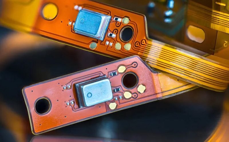
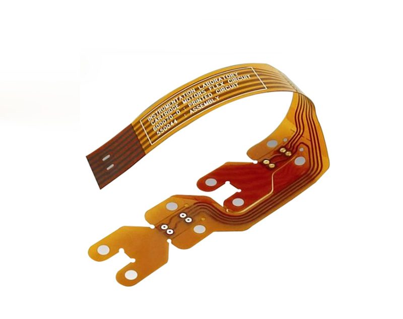
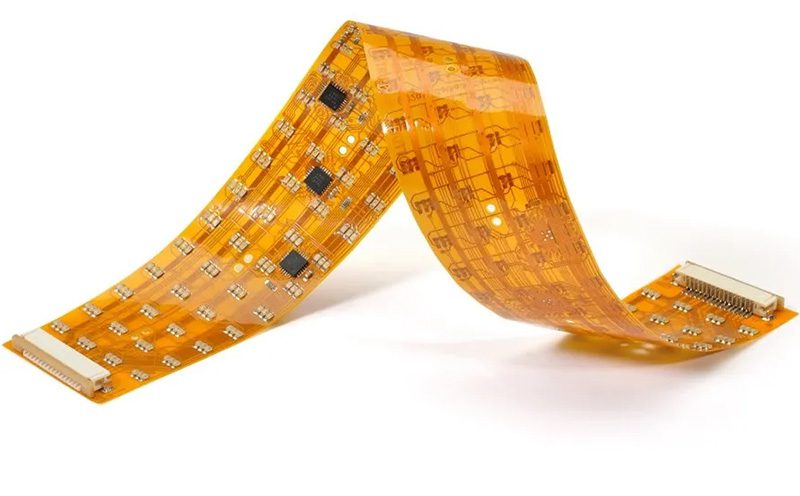
Flexible printed circuit boards (FPC) are bendable circuit boards made of polyimide (PI) or polyester (PET) as the substrate. Unlike traditional rigid circuit boards, FPC are bendable and foldable, requiring more complex manufacturing processes such as material preparation, drilling, electroplating, etching, and peeling. Depending on their structure, flexible circuit boards can be classified as single-sided, double-sided, and multilayer boards, and their appearance can be yellow, black, white, or transparent. With their advantages of being lightweight, thin, and highly flexible, FPC have become an indispensable core component in many precision electronic devices.
Characteristics of flexible PCB
Flexible PCB not only possess excellent flexibility but also boast several unique properties. Compared to traditional rigid circuit boards, flexible PCB typically have lower circuit density and are primarily used for module connections and signal transmission. Because these boards are often used in high-precision equipment, the electronic components used must possess extremely high quality and stability to meet stringent performance requirements.
During assembly, the precision requirements for flexible PCB are particularly demanding—from the strength of solder joints to overall reliability, everything must be strictly controlled to ensure stable operation in complex environments. Although flexible PCB are more expensive than rigid boards in terms of material selection, equipment configuration, and manufacturing processes, their long-term benefits are undeniable.
A carefully designed and rationally laid-out flexible PCB can significantly improve the structural compactness and assembly efficiency of products, thereby optimizing overall production and maintenance costs. With these characteristics, flexible PCB have become a key solution for achieving both high performance and high reliability in modern electronic design.
Considerations for designing flexible PCB
Designing flexible PCB is more challenging than designing rigid PCB, requiring a balance between structural integrity and reliability. The following are key design considerations:
- 1. Via Location
Avoid placing vias in bending or assembly areas to prevent damage during bending or installation. Maintain appropriate spacing and ensure the via diameter matches the board thickness. A via size of around 30μm is generally recommended to improve mechanical strength and reliability.
- 2.Pad and Via Design
Because flexible substrates are bendable and torsion-resistant, pads and vias are more susceptible to mechanical stress. Properly designed pad shapes and via layouts can reduce stress concentration, improve solder joint strength, and enhance electrical performance. Optimized pad design effectively reduces the risk of breakage and extends circuit life.
- 3.Trace Layout
Traces in flexible areas should not overlap between layers to avoid localized stress concentration that could lead to structural deformation or interlayer misalignment. Rounded transitions and teardrop-shaped routing are recommended to reduce interruptions and improve flexibility and stability.
- 4.Copper Layer Design
The copper layer is the core of a flexible PCB, serving both electrical conductivity and overall strength. The design should ensure a uniform copper layer thickness and a well-planned arrangement of copper planes to improve heat dissipation and structural stability. Using solid copper layers helps enhance overall support and bending resistance.
- 5. Spacing Between Drill Holes and Copper Foil
In flexible PCB design, sufficient spacing must be maintained between drill holes and copper foil to avoid stress concentration or copper layer cracking during bending. A proper layout not only improves manufacturing feasibility but also ensures the long-term reliability of the finished product.
Material selection for FPC
The performance and reliability of flexible printed circuit boards (FPC) largely depend on the choice of materials. FPC typically consist of a substrate layer, a conductive layer, and a capping layer.
The substrate layer is often made of polyimide (PI) or polyester (PET). The former offers high temperature resistance and flexibility, while the latter is more cost-effective.
The conductive layer generally uses copper foil, which provides excellent conductivity and high stability; some high-end applications may also use silver paste or conductive polymers.
The capping layer and adhesive are used to protect the circuitry from moisture, oxidation, and mechanical damage.
Different material combinations can achieve a balance between flexibility, heat resistance, and cost depending on the application requirements.
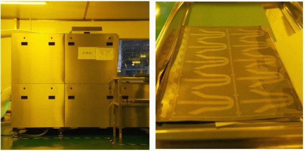
Challenges in processing flexible substrates
Flexible PCB substrates (such as PI and PET) are soft and easily deformable, leading to issues like precision deviations and insufficient adhesion during the initial fixing and cleaning stages of manufacturing.
Regarding substrate fixing, traditional vacuum adsorption methods are prone to stretching deformation. Adopting a “carrier + adhesive fixing” solution effectively improves support, increasing circuit alignment accuracy to ±0.02mm and reducing the offset rate to below 0.5%.
Regarding substrate cleaning and pretreatment, electrostatic adsorption and surface residues can affect plating quality. A combined process of “plasma cleaning + anhydrous alcohol wiping” significantly improves plating adhesion to 1.2N/mm and reduces the cover film bubble rate to 0.5%.
This series of process optimizations effectively overcomes the stability bottleneck of flexible PCBs in the initial manufacturing stage, providing a reliable guarantee for high-precision production.
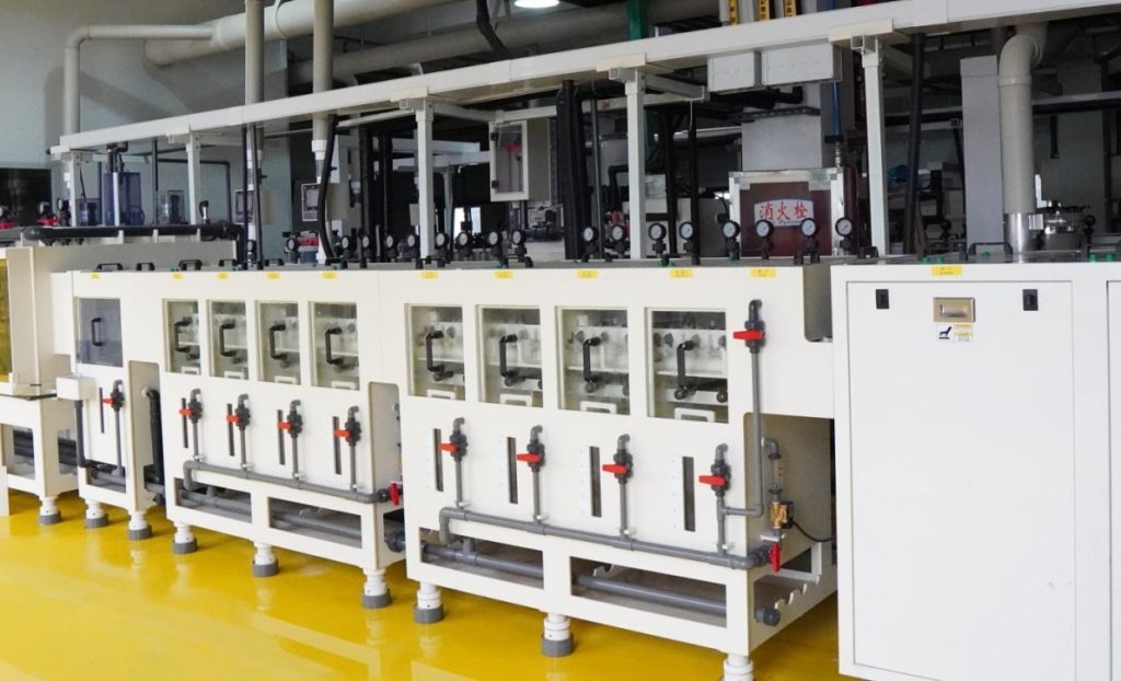
Detailed process of flexible PCB manufacturing
While the manufacturing and assembly of flexible PCB are similar in principle to rigid PCB, their bendable and thin characteristics necessitate more refined production processes and higher requirements for materials, design, and operation. The following is the main process flow for flexible PCB from design to shipment.
- 1.Circuit Fabrication:
After completing the design and material preparation, the first crucial step in flexible PCB manufacturing is the formation of the circuit pattern. Photolithography is typically used to precisely transfer the circuit design to the copper layer surface.
First, a UV-sensitive photoresist is uniformly coated onto a copper-clad flexible substrate. Then, the circuit pattern is exposed to the photoresist layer using a photomask. Areas exposed to UV light solidify, forming a hard structure, while unexposed areas remain flexible. Next, the substrate undergoes a development process, retaining only the photoresist pattern in the solidified areas.
Then, an etching process is performed: the substrate is immersed in an etching solution, dissolving the unprotected copper layer and ultimately leaving the required circuit traces. This process not only determines the accuracy and conductivity of the circuit but also lays the foundation for subsequent via plating, electroplating, and solder mask treatment.
- 2.Lamination and Curing:
Lamination and curing are crucial steps in flexible PCB manufacturing to ensure structural stability and reliability. For multilayer flexible PCBs, multiple flexible core boards need to be precisely stacked and firmly bonded together using a high-temperature, high-pressure lamination process. This process effectively connects different circuit layers, forming a stable overall structure.
After lamination, the flexible PCB undergoes curing, where the adhesives between layers react fully in a controlled high-temperature environment, further enhancing interlayer adhesion and board strength. This step determines the final mechanical stability and long-term reliability of the flexible PCB.
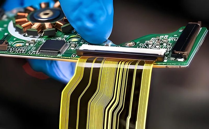
- 3. Drilling and Soldering:
After circuit pattern printing, the flexible PCB manufacturing process enters the critical drilling and soldering stages.
First, drilling is used to create through-holes on the circuit board to connect circuits between different layers and provide a support base for subsequent component mounting. Due to the thinness and susceptibility to heat deformation of flexible materials, traditional mechanical drilling cannot meet high-precision requirements. Therefore, laser drilling is typically used in flexible PCB manufacturing. This method achieves higher hole diameter accuracy and positional consistency while avoiding material damage and ensuring the stability of electrical connections.
Next comes the soldering stage. The main purpose of soldering is to securely mount electronic components onto the circuit board, forming a stable electrical connection. Flexible PCB, due to their thinner structure and different heat dissipation and deformation characteristics, require more stringent soldering processes. Reflow soldering or precision manual soldering is typically used during manufacturing to ensure full solder joints, good conductivity, and to prevent deformation or damage to the flexible material due to overheating, thereby guaranteeing the overall reliability and performance stability of the product.
- 4. Surface Treatment:
In flexible PCB manufacturing, after the circuit pattern is completed, the exposed copper pads must undergo surface treatment to prevent oxidation and maintain good solderability. Surface treatment not only improves soldering quality and corrosion resistance but also extends the PCB’s lifespan. Common flexible PCB surface treatment methods include:
ENIG: A thin layer of gold is deposited on the copper pads, providing excellent soldering performance and corrosion resistance, suitable for high-precision, high-reliability electronic products.
HASL: A uniform layer of tin is deposited on the copper pads. Tin itself has good soldering properties and is relatively inexpensive, suitable for most general-purpose applications.
OSP: A transparent organic protective film is coated on the copper surface to prevent oxidation and maintain good solderability; the process is simple and environmentally friendly.
The surface treatment method for flexible PCB is usually selected based on the product’s application environment, soldering process, and performance requirements. A reasonable surface finish design not only improves the reliability of electrical connections but also provides assurance for subsequent assembly and long-term use.
- 5. Screen Printing and Cutting:
Screen printing is an indispensable and crucial step in flexible PCB manufacturing, typically used to add markings, logos, component numbers, or visual identifiers to the circuit board. During production, the flexible PCB is placed in a screen printing machine, and the pattern is printed onto the white board surface using inkjet or screen printing methods. After completion, the circuit board is baked to cure, ensuring the ink adheres firmly to the PCB surface, guaranteeing clear and durable markings.
Once all circuits and markings are printed, the flexible PCB enters the cutting and shaping stage to obtain the final shape and dimensions. Common cutting methods include:
Die Stamping:This process utilizes a hydraulic punch press and die set to achieve standard straight edges or regular shapes, offering high efficiency, low cost, and suitability for mass production.
Blanking Blade Cutting:This method uses long blades bent to the product contour for cutting, suitable for small-batch production or customized shapes, and can be completed without complex equipment.
Through precise screen printing and high-precision cutting processes, flexible PCB not only ensure functionality but also possess higher aesthetic consistency and reliability, laying a solid foundation for subsequent assembly and applications.
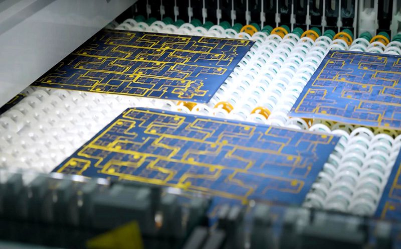
- 6. Inspection and Testing
After the manufacturing process of flexible PCB is completed, the inspection and testing phase before shipment is crucial. To ensure stable product performance and reliable quality, flexible PCB typically undergo multiple rigorous inspections and quality verifications before bending and shaping.
Common inspection items include:
Open and Short Circuit Testing: Confirming the integrity of circuit connections and ensuring there are no potential open or short circuits.
AOI (Automated Optical Inspection): Automatically identifying circuit defects, pad misalignment, or foreign matter contamination using high-precision optical equipment.
Microsection Analysis: Performing microscopic sectioning on samples to inspect the internal lamination structure, hole wall quality, and pad connection reliability.
Visual and Manual Inspection: Final visual and structural verification by experienced inspectors to ensure there is no physical damage or surface defects.
Only after all inspections are completed and quality is confirmed to be acceptable will the flexible PCB enter the cutting, packaging, and shipping process to be delivered to the customer in optimal condition. This rigorous testing process not only ensures product consistency but also reflects the manufacturer’s commitment to the high reliability of flexible circuit boards.
Advantages of flexible PCB over rigid PCB
Flexible PCB, with their thin, light, and bendable characteristics, are becoming a key component in modern electronic product design. Compared to rigid PCB, flexible PCB allow for flexible layouts in space-constrained or structurally complex devices, offering greater design freedom. Their excellent mechanical flexibility, superior heat dissipation, and higher signal integrity make them particularly outstanding in high-performance electronic devices.
In the manufacturing and assembly process, the process flow for flexible PCB is largely similar to that of rigid PCB. However, due to their bendable nature, additional tooling fixtures or auxiliary equipment are typically required to maintain flatness and stability, thereby ensuring soldering quality and overall assembly accuracy. With the continued pursuit of thinner and lighter designs in smart wearable devices, mobile terminals, and high-end electronic products, the market demand for flexible PCB is constantly rising.
Applications of flexible PCB
With the increasing intelligence and miniaturization of electronic devices, the application scope of flexible PCB continues to expand. Besides their widespread use in wearable devices such as smartwatches and health trackers, they are playing an increasingly important role in automotive electronics and medical electronics. For example, in new energy vehicles, flexible PCB are used in movable structures such as rearview mirrors, door controls, and seat adjustments, providing stable and reliable signal transmission. In the medical field, with the rise of implantable monitoring devices and portable diagnostic instruments, flexible PCB have become one of the key connection components.
Furthermore, in Internet of Things (IoT) and smart sensor applications, flexible PCB, due to their high reliability and customizability, have become an ideal choice for supporting dynamic circuits and multifunctional sensing systems. With their superior performance and wide adaptability, flexible PCB are rapidly penetrating various industries, becoming an important trend in future electronics manufacturing.


0 Comments