
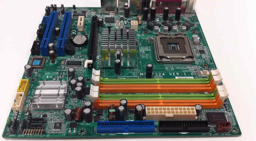
The motherboard is the core and central unit of any computing and automation system. The key functions of a motherboard PCB are to receive input from external sources or memory, process it, generate output, and store it for future reference. Due to complex functionalities and limited product size, motherboard PCBs are typically designed with a multi-layer stack-up structure, which often leads to the question: how many PCB layers does a motherboard have?
When discussing the number of PCB layers, only the copper layers are considered. Other layers, such as solder mask and silkscreen layers, are termed additional layers. The copper layers are arranged in a stacked structure, insulated from each other. Each layer carries power, ground, or signal traces with specific functions. Below is a detailed guide on the typical number of layers in motherboard PCBs, multi-layer stack-up requirements, and layer stacking methods.
Basic Classification of PCB Layers
Printed Circuit Boards can be broadly categorized based on the number of layers as follows:
- Single-layer PCB:
- Has only one conductive copper foil layer; all circuit connections are laid out on this single layer.
- Simple structure, low cost, and mature production process.
- Mainly used in simple electronic devices like basic sensors, toys, and some low-cost electronics.
- Double-layer PCB:
- Has two conductive copper foil layers; circuits are connected through holes (vias).
- Can accommodate more complex circuits, suitable for moderately complex electronic products.
- Commonly used in automotive electronics, household appliances, and communication equipment.
- Multilayer PCB:
- Consists of three or more conductive layers stacked together, with layer counts ranging from 4, 6 layers up to dozens or even hundreds of layers.
- Used in highly integrated, high-speed transmission, and complex signal electronic devices, such as computer motherboards, high-frequency communication equipment, aerospace, and military applications.
- Complex structure, high manufacturing difficulty, and higher cost.
Impact of Layer Count on PCB Performance
- Signal Integrity and High-Speed Transmission:
- Multi-layer PCBs allow for rational arrangement of signal lines with ground or power planes, effectively shielding interference, reducing crosstalk and signal reflection, and ensuring stable high-speed signal transmission.
- High-speed digital and analog signals have high requirements for signal integrity; multi-layer designs provide better electromagnetic compatibility and anti-interference capability.
- Power Management and Voltage Stability:
- Increasing the number of layers provides more power and ground planes, helping to reduce power supply noise and voltage fluctuations, thereby enhancing circuit stability.
- Good power distribution is crucial in high-precision and high-frequency applications.
- Thermal Management:
- Multi-layer PCBs can reasonably arrange thermal layers and heat sinks, improving heat dissipation efficiency, which is particularly important in high-power consumption devices.
- Controlling thermal effects directly impacts device reliability and lifespan.
- Volume and Weight:
- Increasing the number of layers makes the PCB thicker, thereby increasing the device’s volume and weight.
- Layer count optimization is especially critical in mobile devices pursuing lightweight design.
Number of Layers in Motherboard PCBs
The choice of PCB layer count depends on its application scenario. When designing a PCB, it’s essential to select the appropriate number of layers based on actual needs to avoid excessive costs and resource waste.
- Low-End PCBs:
- The simplest circuit designs use a low-end stack-up structure with only 4 layers, which helps beginners understand how many PCB layers are on a motherboard in simpler systems. The top and bottom layers carry signals, while the two inner layers are typically for power and ground. Due to high component density and performance enhancements, this structure is less common in current applications.
- Mid-Range PCBs:
- Many small applications now use motherboards with 6 to 8 layer PCBs, allowing engineers to practically understand how many layers are needed to balance performance and cost. In addition to dedicated internal power and ground layers, this layout includes more signal layers within the internal stack. More layers can also serve as independent power sources for numerous components. The 8-layer PCB stack-up is increasingly popular in most consumer applications due to its design flexibility and better power distribution.
- High-End PCBs:
- Systems containing larger electronic circuits typically use motherboard PCBs with 10 to 16 layers or even more to meet more complex demands. This configuration reflects the number of PCB layers on a motherboard when dealing with advanced designs requiring higher signal integrity. A high PCB layer count allows for effective management of power and signal distribution throughout the PCB stack. Reducing noise, interconnects, and interference becomes more challenging in high-layer-count PCB stacks. The design and manufacture of high-layer-count motherboard PCBs adhere to strict standards.
- Special Cases:
- In critical applications such as advanced computing, defense, space, and telecommunication, where the overall system is too bulky to operate efficiently, engineers need to evaluate the number of PCB layers on the motherboard to achieve extremely high reliability. To meet the demands of such applications, motherboard PCBs can even exceed 20 or 24 layers. The cost of manufacturing such PCBs is very high, requiring extreme care throughout the design and manufacturing process.
Why Motherboard PCBs Need Multiple Layers
f we want to achieve complex applications, the PCB needs to incorporate many functional areas. In such cases, there will be many complex traces and modules on the PCB. However, this sacrifices PCB space, making it unsuitable for many electronic devices. Therefore, to optimize space utilization, the PCB must adopt a multi-layer structure.
- Complex Routing:
- Motherboard PCBs consist of various high-density PTH and SMD components. All these components are interconnected via power, ground, and signal traces. When engineers evaluate the number of PCB layers on a motherboard, they often find it nearly impossible to integrate the entire layout onto a single compact board. Thus, multi-layer layouts are very useful for such applications. Designers can conveniently divide the circuitry into dedicated layers. Furthermore, trace lengths can be effectively shortened, and excessive crossover can be eliminated.
- Power, Ground, and Signal Reference Planes:
- Motherboard PCBs have a high density of electronic components. Most of these components require power and ground connections, and all components need good signal connections. Understanding the number of PCB layers on a motherboard helps designers determine the optimal number of internal layers to ensure power and signal stability. If only a single power and ground source are used in the PCB layout, trace lengths increase, and signal integrity may degrade. To simplify this process, dedicated power and ground planes are set in the internal layers to handle power distribution efficiently. Circuits are divided into groups with similar functions for better signal management.
- Impedance Control and Signal Integrity:
- Impedance control is a critical parameter for high-speed, accurate communication. Understanding how many PCB layers are on a motherboard is crucial because the adjacency between layers directly affects impedance and signal strength. Managing impedance control is more critical due to the involvement of various components. In a multi-layer stack, signal layers are adjacent to power and ground planes to ensure uniform impedance distribution. Maintaining signal integrity throughout the PCB layout is also essential. Traces need to maintain proper spacing and dimensions to avoid signal loss, distortion, interference, and crosstalk.
- Functional Layer Classification:
- The PCB layout can be further divided into sub-areas for classification based on function. These circuit sub-areas can be integrated into internal layers. When analyzing how many PCB layers are on a motherboard, engineers often use this method to optimize electrical performance. To improve work efficiency, some parts can be set in the internal layout. Only the interface parts might need adjustment in the outer areas. Internal vias facilitate proper connections between these layers.
- Manufacturability Within Board Size:
- Manufacturing multi-layer boards is the next crucial step. Any design might seem perfect in theory but may require significant modifications according to manufacturing standards. The manufacturing process becomes more efficient and economical by maintaining a symmetrical or mirrored stack-up. A perfect design should also possess good thermal and mechanical stability during operation. PCBs with an odd number of layers should generally be avoided.
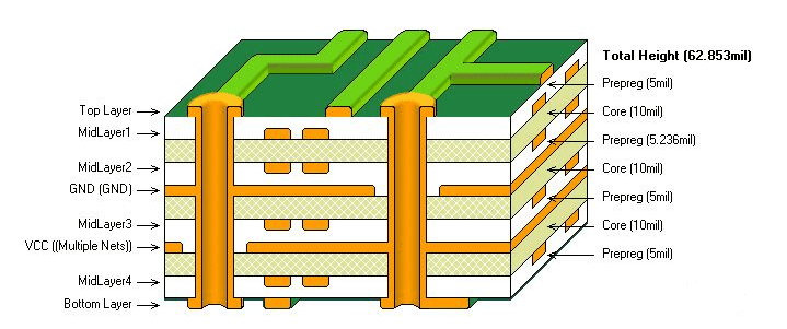
Motherboard PCB Stack-up Methods
A multi-layer board is only useful if all layers are logically arranged. The outer layers (top and bottom) primarily consist of connectors, PTH and SMD components, and a small number of traces. The inner layers are designed to carry power, signals, and ground references as needed. Designers frequently evaluate how many PCB layers are on a motherboard to achieve an appropriate balance between functionality and cost. All these layers are insulated from each other by dielectric layers.
Insulation is crucial for maintaining impedance and signal integrity. Drills are provided for mounting PTH components and connectors. For inner layers, vias (blind or buried) are arranged to enable smoother routing.
Due to the multi-layer layout, each layer requires careful manufacturing and assembly, leading to higher costs. The risk of internal defects, layer-to-layer transfer, delamination, and warping becomes difficult to control. Beyond a certain number of layers, increasing layers necessitates arranging more power and ground reference layers. Therefore, maintaining the minimum number of layers is a challenge when integrating the entire circuit into the PCB designer’s board.
Why is Layer Count So Important?
The increase in layer count is not merely a numbers game; it directly relates to the three core performance pillars of a motherboard:
- Signal Integrity – The “Highway System” of the Digital World:
- Modern computers handle data transfer rates in Gb/s. When signal frequencies reach GHz levels, traces on the PCB are no longer simple “wires” but must be treated as “transmission lines” in microwave engineering. Multi-layer boards allow engineers to use controlled impedance routing methods like “microstrip” and “stripline,” protecting high-speed signals from external interference and preventing them from interfering with others. This directly determines whether memory can run stably at high frequencies and whether PCIe devices can operate at full speed without dropping. Insufficient layers are like running F1 race cars on narrow, unseparated multi-lane roads – frequent accidents are inevitable.
- Power Integrity – The “Heart and Blood Vessels” for Stable Operation:
- CPUs and GPUs are power “monsters” with complex and demanding power requirements. Multi-layer boards allow for the design of low-impedance, low-inductance power distribution networks. Dedicated power and ground planes form a massive “distributed decoupling capacitor” that can instantly respond to the chip’s transient current demands, filtering out minor voltage ripples and drops. A motherboard with insufficient layers may experience significant core voltage fluctuations under high CPU load due to excessive impedance, leading to system instability, performance degradation, or even blue screens.
- Electromagnetic Compatibility and Heat Dissipation – The System’s “Immune and Circulatory Systems”:
- Dense circuits themselves are significant sources of electromagnetic interference. The large-area ground and power planes in multi-layer boards form natural electromagnetic shields, preventing internal signal crosstalk within the motherboard and reducing radiation to external devices, helping pass stringent EMC certifications. Simultaneously, these metal layers are also excellent thermal conductors, able to quickly transfer heat from hot spots like the CPU power delivery module to a larger area of the PCB, acting as a “heat spreader” to aid active cooling.
How to Identify and Weigh the Options?
- How to Determine How Many Layers My Motherboard Has?
- Official Specifications Sheet: The most authoritative method. However, manufacturer strategies vary; high-end models are more willing to specify, while low-end and mid-range models often remain vague.
- Observe the Motherboard Edge: Look carefully at the motherboard’s cross-section. If visible, you might see distinct copper layer markings. However, modern motherboards often have ink or plating covering the edges, making observation difficult.
- “Through-Hole” vs. “Blind/Buried Vias”: If a hole goes straight from the top to the bottom layer, it doesn’t indicate the total layer count. However, if you see holes that don’t penetrate fully, connecting only surface or inner layers, these are typically signs of high-end boards with 8 layers or more, as this high-cost technique maximizes routing space utilization.
- Price and Positioning: This is the most practical judgment method. A motherboard below a certain price point is almost certainly not above 8 layers; whereas flagship boards are typically 10 layers or more. Often, for the same chipset, a higher price usually correlates with more layers.
- Are More Layers Always Better? – A Rational View of the “Arms Race”:
- Theoretically yes, but we need to be rational, considering cost and actual needs.
- Soaring Costs: For every two layers added, the PCB’s raw material cost, processing difficulty (drilling, alignment, lamination yield), and design cycle increase exponentially.
- Design is the Soul: Layer count provides the stage, but excellent routing design, component selection, and firmware tuning are the performers on that stage. A poorly designed 10-layer board might be worse than a well-designed 8-layer board.
- Law of Diminishing Returns: For average users who don’t overclock and only use mainstream hardware for daily tasks, the practical experience gain from upgrading from a 6-layer to a 10-layer board is minimal. The performance bottleneck is more likely to be the CPU, graphics card, or hard drive, not the motherboard’s traces. Allocating budget to these components often yields higher returns.
Design Considerations
- Cost and Manufacturing Difficulty:
- Higher layer counts increase manufacturing complexity and cost.
- Multi-layer boards require multiple lamination, drilling, and alignment steps, demanding high process standards.
- Design Layout:
- The stack-up structure should be reasonably arranged to ensure the shortest signal paths and reduce interference.
- Symmetrical stack-up structures are typically used to minimize thermal deformation and mechanical stress.
- Reliability:
- Multi-layer PCBs must ensure insulation quality and connection reliability between layers, avoiding voids and layer separation issues that affect electrical performance.
- Strict testing and quality control are key to ensuring the reliability of multi-layer boards.
- Electromagnetic Compatibility:
- Multi-layer design helps achieve good EMC, complying with modern electronic device regulations.
- Design must consider the layout of shielding layers and signal layers.
Summary
Motherboards in modern electronic devices employ multi-layer structures, with layer counts varying from small to large. Higher layer counts can improve routing flexibility, signal integrity, and power distribution efficiency. However, this also increases overall cost, complexity, and manufacturing risk.
Therefore, understanding the number of PCB layers on a motherboard has become an important consideration in early design evaluation. Determining the total number of layers for any device’s motherboard is always a critical task.
As product functionalities continue to increase and end-product structures become more compact, motherboard PCB manufacturing has also become more complex, with many new trends emerging in this field.


0 Comments