
The printed circuit board (PCB) is the core component of modern electronic devices. Nearly all electronic products rely on it, from simple electronic watches to complex computer systems. Printing PCB boards for manufacturing is a complex and precise process involving multiple specialized steps and strict quality control.
This article details the complete PCB manufacturing workflow, the characteristics of different manufacturing techniques, material selection considerations, and quality control methods, providing a comprehensive understanding of how to successfully print PCB boards for manufacturing.
Basic Concepts and Importance of PCB Manufacturing
PCB manufacturing refers to the entire process of creating printed circuit boards, which are essential components in electronic devices, providing electrical connections between various electronic components (such as integrated circuits, resistors, capacitors, and connectors).
The quality of PCB manufacturing directly affects the performance, reliability, and lifespan of the final electronic product. Therefore, mastering the correct PCB printing methods is crucial for electronic product development.
Types of PCB Manufacturing
A PCB unit contains many elements that constitute the final product. A typical PCB structure includes layers, component pads, interconnection traces, solder mask, silkscreen, PTH and SMD components, vias, drill holes, and other required materials. Understanding PCB design concepts helps ensure the integrity of the printing process for complete manufacturing and explains how to print a PCB board. PCB manufacturing processes are primarily divided into two types. Each process requires a printable layout for further component assembly and PCB manufacturing.
DIY Fabrication
Preparing PCB boards locally using limited resources and mechanical equipment is known as DIY (Do-It-Yourself) fabrication. This method allows for rapid PCB board production, enabling beginners to learn how to print PCB boards. It is suitable for small-batch applications. Despite its limitations, the DIY approach is still used by new product development teams and small PCB production units because automated manufacturing processes are often too costly for such small projects.
Standard Manufacturing
Over the years, PCB manufacturing units have evolved into standardized configurations with greater technical expertise to achieve high yield, improved efficiency, and the ability to handle complex applications. The standard PCB manufacturing method ensures consistent, high-quality output and provides guidance on how to print PCB boards. Establishing a standard automated PCB manufacturing and assembly process requires significant process investment. Due to standard configuration and running costs, this method is not suitable for custom and low-volume production.
Complete Process Flow of PCB Manufacturing
- Circuit Layout Design: The first step in PCB manufacturing is designing the circuit layout using ECAD (Electronic Computer-Aided Design) software. After the design is complete, the layout data is converted into Gerber files, which contain all necessary information including copper layer coordinates, solder mask, silkscreen, drill data, etc.
Finally, the design’s manufacturability is verified through Design Rule Check (DRC).
Pre-Production Preparation
- Printing Films: High-resolution negatives for each layer are printed onto transparent plastic sheets coated with photosensitive emulsion using specialized photoplotter printers. Registration holes on these films ensure precise alignment between layers.
- Copper Clad Laminate Preparation: The raw PCB substrate is cleaned and laminated with a photoresist layer. Sometimes, adhesion promoters are used to help the resist bond better.
Pattern Transfer and Etching
- Selective Exposure: The negatives are precisely aligned with the laminated board using registration pins, and then the photoresist is selectively exposed to a UV light source according to the layer image.
- Developing and Etching: The board is immersed in a chemical developer solution to dissolve the unexposed resist. Then, an etchant is used to remove the copper not protected by the resist, forming the conductor pattern.
- Stripping: The dry film photoresist protecting the copper surfaces is completely stripped using a sodium hydroxide solution, exposing the circuit pattern.
Multilayer Board Processing
- Lamination: For multilayer PCBs, the individual inner and outer layers need to be aligned using registration holes or vision systems. Prepreg and copper foil are then precisely stacked and laminated together under heat and pressure.
- Drilling: Precision CNC drilling machines are used to drill holes for component leads and vias connecting the layers. The hole walls are then deburred.
- Plating: A thin copper layer is formed on all exposed surfaces through autocatalytic deposition, providing a conductive base for electroplating, enabling current flow between layers.
Post-Processing
- Solder Mask Application: A liquid photo-imageable solder mask is applied to the entire board and cured to protect the copper traces from oxidation and prevent solder bridges.
- Surface Finish: A surface finish is applied to the exposed copper. Common methods include Hot Air Solder Leveling (HASL), Organic Solderability Preservative (OSP), Immersion Silver, or Immersion Gold (ENIG).
- Silkscreen Printing: Ink is used to print reference designators, symbols, company information, board outlines, and other markings, typically using screen printing.
Testing and Inspection
- Electrical Test: Verification for the absence of opens or shorts is performed via continuity, isolation tests, and In-Circuit Test (ICT) or Flying Probe Test.
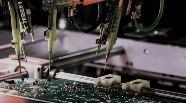
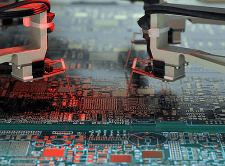
- Automated Optical Inspection (AOI): High-definition image cameras quickly capture images of the board, which are compared with the original design data to fundamentally identify potential issues like shorts and opens.
- Final Quality Inspection: Electrical, visual, and mechanical inspections are conducted to ensure the board meets specifications before shipment.
Main Technical Methods in PCB Manufacturing
Amateur Fabrication Methods
- Perfboard and Breadboard: This is the simplest method of PCB fabrication, using boards with holes drilled at 2.54mm spacing on hard paper or epoxy. Components are inserted from the non-copper side and soldered on the other side. This method is suitable for quickly setting up simple circuits but cannot meet long-term or complex needs.
- Milled Circuit Boards: A small milling machine is used to mill conductor paths on a copper-clad board. This method allows for long-term use but quickly reaches its limits with complex PCBs and requires operator skill.
- Etched Circuit Boards: Circuit traces are formed by selectively removing copper from the substrate. First, the circuit layout is mapped onto the copper laminate, then the traces are protected using a resist material, and finally the board is immersed in an etchant solution to remove unwanted copper.
- Toner Transfer Method: A laser printer is used to print the mirrored layout onto coated paper. Heat and pressure are then applied to transfer the toner onto a cleaned copper board, creating a resist pattern for etching.
Professional Manufacturing Services
Professional PCB manufacturing services use advanced processes like photolithography to produce industrial-grade circuit boards with fine features. This method is suitable for mass production or complex multilayer boards, providing high-quality, production-grade PCBs.
Partnering with a reliable PCB manufacturer is crucial, as even the smallest error can lead to costly consequences.
PCB Material Selection
The following are common substrate types:
- FR-4 Epoxy Glass Fiber Substrate: This is the most widely used PCB substrate material today, using glass fiber cloth as the reinforcement and epoxy resin as the binder. FR-4 offers good mechanical strength, electrical insulation, heat resistance, and cost-effectiveness, making it suitable for most general-purpose electronics.
- High-Frequency & High-Speed Materials: Used in technologies like 5G communication, data centers, and radar, these materials require lower signal transmission loss. They typically use special resins (e.g., PTFE, PPE) and low-Dk glass fabric to achieve lower dielectric constant and loss.
- Metal Core Substrates: Primarily used in applications requiring efficient heat dissipation, such as LED lighting and high-power supply modules. They usually consist of a metal base (e.g., aluminum, copper) and an insulating layer, utilizing the metal’s thermal conductivity to dissipate heat.
- Flexible Materials: Materials used for Flexible Printed Circuits (FPC), mainly including Polyimide (PI) film and Polyester (PET) film. These materials offer excellent flexibility, enabling product bending and folding, and are suitable for wearable devices, foldable screen phones, etc.
PCB Printing Methods
Toner Transfer (Laser Printer) Method
This is a simple method commonly used in the DIY fabrication process. First, the circuit layout is printed onto glossy paper, making it a practical example for PCB board printing. The glossy paper is then placed on the copper layer of the PCB and pressed with a heated iron. This process transfers the layout from the glossy paper to the bare board. The printer ink remains unaffected during etching and is removed afterwards to reveal the circuit layout. This method is simple and low-cost but not suitable for fine-pitch components. The Toner Transfer method also has lower precision.
UV Exposure
For complex circuit layouts requiring high precision and standard surface finish, UV exposure (photoresist) is another option for PCB printing. The layout is printed onto a transparent film and placed on the bare board, demonstrating how to print a PCB board for advanced applications. This stack is then exposed to UV light. The UV light reacts with the photoresist in the transparent areas of the film, while the areas under the printed layout remain unaffected. The board is then washed with a cleaning chemical to remove the unwanted copper.
Overview of the PCB Printing Process
The entire PCB printing process involves both design and fabrication. We need to confirm that the PCB design meets practical manufacturing requirements. Any defects in the design stage can impact the PCB printing process, leading to non-conforming final products. Below is the PCB printing workflow.
PCB Design
Any PCB manufacturing starts with a detailed design process. The circuit needs to be carefully transferred onto the PCB. When converting the schematic into a physical layout, components and routing must be placed meticulously. Sufficient spacing and dimensions must be set to maintain circuit performance.
The circuit must be correctly divided into layers with proper connectivity. All types of errors must be checked using DRC functionality. Gerber files must contain detailed information for all layers, solder mask, silkscreen, drill data, pads, and component details. After the PCB layout is completed and verified, the final output package is prepared for the further manufacturing process, considering how to effectively print the PCB board.
Design Printing
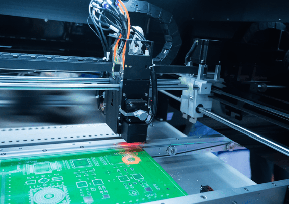
The PCB substrate uses pure copper cladding. The circuit is printed onto it. Any suitable method can be used to print the circuit onto the PCB board; this article explains how to print a PCB board for actual production. Please use standard Gerber files or the design package to print the PCB. Board dimensions, thickness, copper foil thickness, and all parameters must meet the final requirements. Printing must be done at the highest possible resolution.
Board Etching
After the circuit is printed onto the copper board, the excess or unwanted copper needs to be removed. The board is immersed in water to remove contaminants. Then, the print quality on the board is carefully inspected. Any damaged or untouched areas must be repaired through separate marking and covering. Next, the board is placed in a dedicated chemical solution for etching until the exposed copper completely disappears.
Finally, the board is thoroughly rinsed and dried. During the etching and rinsing process, no part of the circuit should be removed. The board must undergo visual and electrical inspection to ensure smooth circuit transfer, keeping in mind how to correctly print the PCB circuit board.
Board Finishing
Drill holes, slots, or vias (blind or buried) are created on the etched board according to the PCB layout. Solder mask is applied, followed by surface finish. For better component identification and PCB details, a silkscreen layer is also printed on the PCB, demonstrating how to print a PCB board clearly. The board is cleaned with Isopropyl Alcohol (IPA) to remove any unwanted elements. Now, the PCB is ready for further component assembly.
Quality Control in PCB Manufacturing
Process Quality Control
- SPI (Solder Paste Inspection): Utilizes 2D/3D solder paste inspection machines to detect all or critical solder paste application points, extracting and recording paste parameter values. This allows timely discovery of printing quality defects and reduces the spread of non-conforming products.
- AOI (Automated Optical Inspection): Primarily used to inspect defects related to solder paste printing, component placement, and soldering. A CCD automatically scans the board and captures images, then the collected data is compared with pre-recorded parameters to determine consistency in features like solder joints and components.
Finished Product Testing
- ICT (In-Circuit Test): Primarily tests for open circuits, short circuits, and the soldering condition of all components on a PCBA by using test probes to contact test points on the board.
- FCT (Functional Test): After programming, the PCBA board is connected to loads, simulating user input and output to achieve software-hardware co-debugging and confirm the front-end manufacturing and soldering conditions.
- Aging Test: The PCBA board is placed under specific temperature and humidity conditions for prolonged powered-on testing, simulating user usage to detect issues like cold solder joints and poor connections.
- Environmental Testing: The PCBA is subjected to harsh environmental conditions, such as high temperature, low temperature, and drop tests. The results from these tests are used to evaluate the reliability of the PCBA board.
Standards and Specifications for PCB Manufacturing
PCB manufacturing follows various industry standards, including:
- IPC Standards: Standards for the electronics manufacturing industry developed by the Association Connecting Electronics Industries, covering all aspects of PCB design, manufacturing, and assembly.
- UL Certification: Certification services for PCBs provided by Underwriters Laboratories, ensuring they meet safety and performance standards.
- ISO Standards: Relevant standards from the International Organization for Standardization, including ISO 9001 and ISO 14001, pertaining to quality control and environmental management.
- RoHS and REACH Compliance: Regulations restricting the use of certain hazardous substances in PCBs and electronic products.
Conclusion
Printing PCB boards for manufacturing is a complex and precise process involving design, material selection, various processing techniques, and strict quality control. As electronic devices trend towards miniaturization and high performance, the requirements for PCB manufacturing processes are becoming increasingly demanding.
Whether choosing amateur fabrication methods or professional manufacturing services, a comprehensive understanding of the entire process is necessary to ensure the production of high-quality, reliable printed circuit boards. By mastering the basic principles, process flow, and quality control methods of PCB manufacturing, you will be better equipped to plan and execute PCB printing projects, laying a solid foundation for electronic product development.


0 Comments