
Introduction
Electronic prototyping boards are indispensable tools in the modern electronics product development process, serving as a bridge between conceptual design and the final product. In today’s fast-paced technological innovation environment, companies face immense pressure to rapidly transform ideas into tangible products. Electronic Prototyping Boards are key tools meeting this demand. According to market analysis reports, the global electronic prototyping market size reached hundreds of billions of RMB by 2024 and is expected to maintain steady growth until 2030. This data fully demonstrates the significant role of electronic prototyping boards in the field of electronic product development.
Electronic prototyping boards are widely used in various sectors such as consumer electronics, automotive electronics, industrial control, and IoT devices. For startups and hardware entrepreneurs, electronic prototype design is a crucial step for establishing proof of concept and securing funding. The prototyping phase allows for cost assessment, testing of various ideas and solutions. In large tech companies, prototype verification becomes a core part of controlling time-to-market for chips and optimizing development processes. Particularly in the semiconductor industry, prototype verification helps engineers validate design correctness before tape-out, significantly reducing development risks and costs.
When using electronic prototyping boards, engineers need to comprehensively consider several factors: first is project complexity – a simple sensor circuit might only require a basic breadboard, whereas a complex SoC design might need a multi-FPGA commercial prototyping system; second is the development stage – early proof-of-concept suits breadboards requiring no soldering, while near-product prototypes need custom PCBs; and team resources, including technical support capabilities, time constraints, and budget conditions. Understanding these considerations helps select the most suitable electronic prototyping board for project needs, avoiding common development pitfalls and improving product development efficiency.
What is an Electronic Prototyping Board?
An electronic prototyping board, also known as a prototype development board or prototype verification platform, is a specialized tool used for building and testing electronic circuits. It provides a physical platform enabling engineers to transform conceptual circuit designs into functional prototype systems, thereby validating design functionality, reliability, and performance. From a technical perspective, electronic prototyping boards typically include basic components such as an insulating substrate, interconnection system, power distribution network, and input/output interfaces, forming a complete circuit verification environment.
The development of electronic prototyping boards has undergone a long evolution. The earliest electronic prototyping used wooden boards (like cutting boards) as bases, with components fixed by screws and nails as connection points. With the advancement of electronic technology, solderless breadboards emerged in the 1970s, using spring clip connections, greatly improving prototyping efficiency. Entering the 21st century, the proliferation of surface-mount technology drove the development of more professional prototyping boards, including various development kits and commercial prototype verification systems. Recently, with increasing chip complexity, multi-FPGA prototype verification systems and high-density interconnect prototyping boards have become mainstream choices for complex SoC verification.
Electronic prototyping boards play a vital role in the product development流程. Generally, electronic product development goes through multiple stages: “Proof of Concept → Functional Prototype → Engineering Prototype → Production Prototype”. Electronic prototyping boards are widely used in the early stages: during the Proof of Concept stage, engineers use breadboards or basic prototyping boards to quickly test circuit ideas; in the Functional Prototype stage, more stable prototyping boards are used to verify core functions; in the Engineering Prototype stage, custom PCB prototypes close to the final product form are used for system verification. This gradual prototyping approach effectively reduces development risks, identifying and resolving design issues before mass production.
Taking smart home device development as an example, engineers might first use Arduino and breadboards to build a proof-of-concept prototype, validating sensor response algorithms; then move to custom PCB prototyping boards, integrating optimized circuit designs and communication modules; finally create engineering prototypes to test the product’s actual performance and user experience. Through this series of prototype iterations, companies can bring reliable products to market with minimal cost and maximum speed.
Main Types of Electronic Prototyping Boards in the Market and Their Technical Specifications
Electronic prototyping boards in the market can be categorized into various types based on complexity, application scenarios, and technical characteristics. Each type has specific technical specifications and suitable domains. Understanding these categories and their features is crucial for selecting the most appropriate electronic prototyping board for project needs.
1 Breadboard (Solderless Protoboard)
Breadboards are the most basic and common electronic prototyping boards, especially suitable for educational scenarios and simple circuit verification. Modern solderless breadboards typically consist of multiple insertion holes and internal metal spring clips, forming a standard 0.1-inch (2.54mm) grid system. For example, the Bud Industries BB-32621 breadboard, measuring 3.2 inches × 2.08 inches, contains 400 connection points (300 for component connections, 100 for power distribution). Such breadboards usually have horizontal power rails along the long edges for distributing positive and negative power, with short vertical connection strips in the central area for component connections.
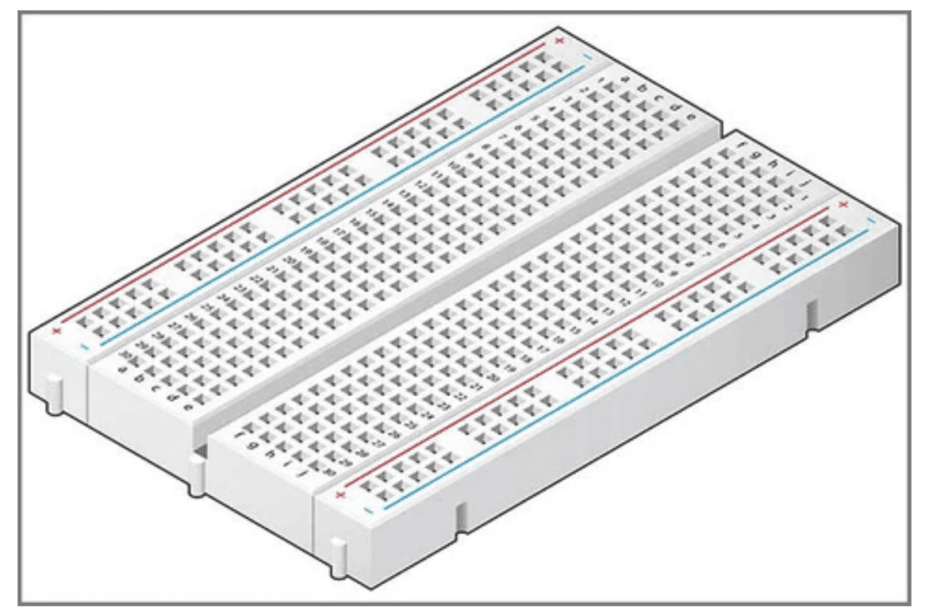
Breadboards are primarily suitable for preliminary verification of low-frequency signal circuits (typically below 10MHz) and digital logic circuits. Due to their solderless nature, engineers can quickly modify circuit structures, making them ideal for iterative design processes. However, breadboards have significant parasitic inductance and capacitance, making them unsuitable for high-frequency RF circuits or high-speed digital designs. For surface-mount devices (SMD), additional adapter boards are usually needed, such as the Logical Systems PA-SOD3SM18-16 adapter, which converts SOIC-packaged ICs to a 0.1-inch DIP package suitable for breadboards.
2 Prototype Board (Soldered Protoboard)
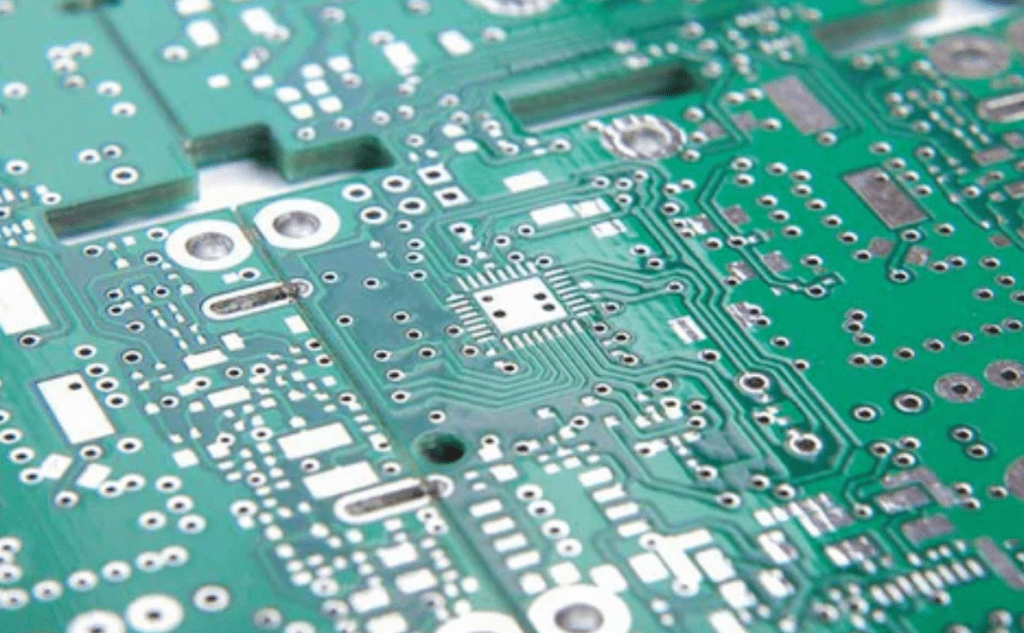
Prototype Boards provide a more stable and durable prototyping solution, consisting of an insulating substrate (typically FR4 epoxy glass) and regularly arranged pads or through-holes. The Bud Industries EXN-23404-PCB is a typical prototype board, measuring 4.02 inches × 3.87 inches, with a thickness of 1.6mm, featuring plated through-holes with a diameter of 1.3mm and a center spacing of 2.54mm. Unlike breadboards, prototype boards require soldering to fix components and establish electrical connections, making them more suitable for medium to long-term projects or applications requiring mechanical stability.
Prototype boards can be divided into general-purpose and special-purpose categories. General-purpose prototype boards provide standard pad arrays, allowing engineers to customize interconnections according to circuit requirements; special-purpose prototype boards are pre-designed with partial circuits for specific applications, such as power management, signal conditioning, or specific interfaces. Prototype boards can handle more complex circuit designs and, through careful layout, can be used for medium-frequency (tens of MHz range) analog and digital circuits. Due to the ability to use short wire connections and ground planes, prototype boards have far better parasitic parameters than breadboards, offering improved signal integrity.
3 Commercial Prototype Verification Systems
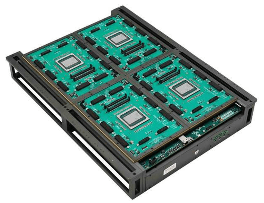
For the most complex chip and system-level designs, Commercial Prototype Verification Systems provide complete and highly specialized solutions. These systems typically consist of multiple large-capacity FPGA chips, rich interface resources, and professional software toolchains. For example, the S2C Prodigy series prototype verification systems support single, dual, quad, and even octa-core configurations, and can be expanded through cascading up to 256 FPGAs. Such systems can support circuit capacities up to tens of billions of gates, meeting the most complex SoC design and verification requirements.
The technical specifications of commercial prototype verification systems are extremely advanced: supporting signal transmission rates up to 25Gbps, providing a 8K:1 time-division multiplexing ratio, and equipped with comprehensive automatic partitioning and parallel compilation tools. These systems usually come with abundant peripheral interface daughter cards; for instance, S2C offers over 90 different daughter cards and accessories, covering mainstream application areas like Arm processor interfaces, embedded systems, and multimedia modules. Furthermore, professional debugging solutions like MDM Pro support multi-FPGA collaborative debugging, providing sampling frequencies up to 125MHz and maximum 64GB DDR memory for waveform storage, greatly enhancing debugging efficiency for complex systems.
Table: Comparison of Main Electronic Prototyping Board Types and Technical Parameters
| Prototyping Board Type | Suitable Circuit Scale | Typical Signal Frequency | Connection Method | Main Application Scenarios |
|---|---|---|---|---|
| Breadboard | Small circuits (<100 components) | <10MHz | Spring clip contacts | Education, simple circuit verification |
| Prototype Board | Small to medium circuits | <100MHz | Soldered connections | Medium-term projects, functional verification |
| Commercial Prototype Verification System | Very large-scale SoC | >1GHz | High-speed interconnect | Chip verification, system development |
Besides the three main categories above, there are numerous development boards targeting specific platforms or applications, such as the Renesas Electronics RL78 Rapid Prototyping Board. This board is specifically designed for RL78/G14 and RL78/G1D 16-bit microcontrollers, including emulation circuits and various connection interfaces (USB, Pmod, and Arduino), allowing developers to quickly evaluate MCU performance without designing dedicated hardware. Such evaluation boards are extremely useful in embedded system development, significantly shortening the initial verification cycle.
Advantages and Disadvantages of Different Categories of Electronic Prototyping Boards
Understanding the advantages and disadvantages of various electronic prototyping boards is crucial for making correct technical selections. Different categories of prototyping boards have significant differences in connection stability, reconfigurability, applicable scenarios, and overall cost, which directly impact development efficiency and project success.
1 Advantages and Limitations of Breadboards
The primary advantage of breadboards is their solderless connection characteristic, allowing engineers to quickly modify circuit designs, replace components, or adjust connections without desoldering. This feature makes breadboards ideal platforms for circuit learning, proof of concept, and preliminary debugging. For beginners, breadboards significantly lower the entry barrier, enabling circuit experiments without soldering skills. Furthermore, the visual layout of breadboards allows engineers to clearly observe all connections, aiding in understanding circuit operation principles and troubleshooting.
However, the limitations of breadboards are also evident. Their spring clip connection method leads to poor mechanical stability; over time and with repeated insertions, connection points can loosen, causing intermittent faults. The electrical characteristics of breadboards are also not ideal; higher parasitic inductance and capacitance make them unsuitable for high-frequency applications, while contact resistance can affect precision measurement circuits. Additionally, the predefined connection patterns of breadboards limit layout flexibility, and complex multi-component circuits often become messy, difficult to manage and debug.
2 Advantages and Limitations of Prototype Boards
Prototype boards provide a highly stable and reliable circuit platform through soldered connections. The mechanical and electrical connections formed by soldering can withstand vibration, temperature changes, and the test of time, suitable for long-term use and final product integration. Prototype boards offer extremely high layout flexibility, allowing engineers to optimize component placement and trace routing according to circuit requirements, supporting complex multi-component designs. By using ground planes and shielding techniques, prototype boards can handle higher frequency analog signals and high-speed digital logic.
The main disadvantage of prototype boards is their difficulty of modification. Each circuit change requires desoldering and resoldering, a process that is time-consuming and may damage the board and components. Using prototype boards also requires additional skill investment; engineers must master professional soldering techniques and PCB design knowledge. Although the cost of prototype boards themselves is not high, the配套 tools (soldering stations, debugging equipment, etc.) and time investment increase the overall cost. Furthermore, homemade prototype boards are usually limited to simple designs; complex multilayer boards still require professional manufacturer fabrication, increasing iteration cycles.
3 Advantages and Limitations of Commercial Prototype Verification Systems
Commercial prototype verification systems excel in handling very large-scale circuits, particularly suitable for complex SoC verification and software development. These systems provide massive FPGA capacity and high-speed interconnection, supporting performance verification in real environments. The automated toolchains of commercial systems (such as automatic partitioning, parallel compilation) significantly reduce engineering burden, while rich interface libraries and debugging solutions accelerate system integration and problem identification. Furthermore, market-proven commercial systems (like S2C Prodigy) provide reliable performance and extensive technical support.
The main limitation of commercial systems lies in their high cost, which may be prohibitive for budget-limited projects or small teams. System complexity also brings a steep learning curve, requiring specialized training for engineers to use effectively. Although commercial systems support large-scale designs, configuring and optimizing multi-FPGA partitions still requires professional knowledge; improper partitioning may lead to performance bottlenecks and debugging difficulties. Additionally, general-purpose commercial systems may not fully meet the special requirements of specific applications, requiring a balance between performance and flexibility.
Table: Comparison of Key Features of Different Electronic Prototyping Board Categories
| Characteristic | Breadboard | Prototype Board | Commercial Prototype Verification System |
|---|---|---|---|
| Connection Stability | Low, relies on spring clips | High, soldered connections | Very high, professional-grade connections |
| Reconfigurability | High, no soldering required | Low, requires desoldering | Medium, configurable via software |
| Circuit Complexity | Simple to medium | Simple to complex | Extremely complex, supports SoC-level |
| High-Frequency Performance | Poor, large parasitic parameters | Medium, can be optimized | Excellent, professionally designed |
| Initial Cost | Low | Medium | High |
| Skill Requirements | Low | Medium to High | High, requires professional training |
4 Advantages and Limitations of Specialized Development Boards
Besides the above three categories, there are various specialized development boards (such as Arduino, Raspberry Pi, etc.), which have unique advantages in rapid prototyping and ecosystem support. These development boards provide complete hardware platforms and rich software libraries, greatly lowering the development threshold for specific application areas. However, these development boards face challenges when transitioning to production; their economy and efficiency are not advantageous in mass production, usually requiring a shift to custom PCB designs for cost optimization and space reduction.
Common Mistakes When Using Electronic Prototyping Boards and How to Avoid Them
During the electronic prototyping process, engineers, especially beginners, often make some typical mistakes. These errors can range from causing abnormal prototype functionality to component damage or project delays. Recognizing these common mistakes and understanding preventive measures is key to improving prototyping success rates.
1 Circuit Design and Layout Errors
Improper Power Management is one of the most common and harmful mistakes. Many engineers focus on signal circuit design but neglect power distribution system optimization. Typical manifestations include: neglecting the use of decoupling capacitors, using overly thin power traces, improper ground loop design, etc. These oversights can lead to voltage drops, noise coupling, and system instability. The solution is to add appropriate decoupling capacitors at key circuit nodes (especially near IC power pins), use star or plane grounding strategies, and provide separate power paths for high-power-consumption components.
Neglecting Signal Integrity is another common mistake, especially in high-speed digital circuits or analog circuits. Attempting high-frequency designs on breadboards, using excessively long connecting wires, ignoring impedance matching—all can lead to signal distortion. For high-frequency signals, prototyping boards with low parasitic parameters (like prototype PCBs with ground planes) should be selected, signal paths should be kept short, and terminal matching resistors should be used. For sensitive nodes like clock signals, shielding and protection measures should be employed to prevent crosstalk and radiation.
Insufficient Circuit Testing is also a common issue. Many engineers directly integrate complete systems without verifying subsystems, making fault localization difficult. The correct approach should adopt progressive verification, independently testing each functional module first, confirming normal operation before system integration. Use tools like oscilloscopes and logic analyzers to comprehensively verify waveforms at key nodes, ensuring they meet design expectations.
2 Prototyping Board Selection and Usage Errors
Mismatch between Prototyping Board and Development Stage leads to inefficiency or resource waste. Common mistakes include: using soldered prototype boards in the early exploration stage (difficult to modify), or still using breadboards in the near-product stage (poor stability). The appropriate prototyping board should be selected based on the development stage: proof of concept uses breadboards, functional verification uses soldered prototype boards, system verification uses commercial verification systems or custom PCBs.
Ignoring Physical Limitations also causes problems. Each prototyping board has its limitations: breadboards are unsuitable for high-power devices (causing contact point overheating), ordinary prototype boards are unsuitable for microwave frequencies (causing significant signal loss), single-FPGA systems may not accommodate complex designs. Engineers should understand the limits of the chosen platform and promptly upgrade to a more suitable platform when capabilities are exceeded. For complex designs, consider using multi-FPGA partitioning and automatic partitioning tools.
Insufficient Thermal Management is particularly common in power electronics prototypes. Engineers often underestimate component power dissipation, leading to prototype board overheating and performance degradation. For power components, adequate heat dissipation measures should be provided, such as heat sinks, ventilation holes, or even forced cooling. Simultaneously, pay attention to current density, avoiding using overly thin wires or traces to carry large currents.
3 Tool Usage and Project Management Errors
Improper Debugging Methods can significantly extend development cycles. Common mistakes include: lacking systematic debugging strategies, over-relying on a single debugging tool, neglecting logs and data analysis. Effective debugging should proceed from global to local: first confirm power and clock normality, then check control signals, finally verify data paths. Combine multiple debugging tools simultaneously, such as hardware debuggers, logic analyzers, and software diagnostics, fully utilizing professional debugging solutions provided by commercial prototype verification systems, like S2C’s MDM Pro supporting multi-FPGA collaborative debugging.
Project Management Errors similarly affect prototyping efficiency. Prematurely Building Prototypes without sufficient thought and planning is a typical mistake. Before starting prototypes, clearly define test objectives and verification criteria, establish detailed timelines and resource allocation. For team projects, establish clear documentation and version control to avoid confusion and duplicate work. Regularly conduct design reviews and progress assessments, ensuring prototype development proceeds as planned and adjusting strategies promptly.
About General Electronic Prototyping Boards
Selecting a general electronic prototyping board is a comprehensive decision-making process, requiring engineers to evaluate the most suitable solution based on project requirements, resource constraints, and technical objectives. Correct selection can accelerate development cycles, reduce development costs, and improve final product quality.
1 Key Factors in Electronic Prototyping Board Selection
When selecting an electronic prototyping board, engineers should comprehensively consider multiple factors:
- Project Stage Suitability: Early proof-of-concept requires highly flexible platforms (like breadboards), while system verification requires highly stable platforms (like custom PCBs or commercial verification systems). Using highly polished prototypes in early stages can be counterproductive, as it limits iterative flexibility and adds unnecessary development burden.
- Circuit Complexity and Scale: Simple circuits (less than 100 components) can use breadboards or basic prototype boards, medium-complexity designs (100-1000 components) require soldered prototype boards or standard development boards, while highly complex SoC designs (tens of millions of components) must use multi-FPGA commercial prototype verification systems.
- Signal Performance Requirements: Low-frequency DC circuits (sensors, control interfaces) can be implemented on breadboards, medium-frequency analog and digital circuits (audio, video processing) need prototype PCBs, high-frequency RF or high-speed serial interfaces (PCIe, DDR) must use professional prototyping boards with impedance control and shielding design.
- Team Resources and Skills: Assessing the team’s technical capabilities is crucial. If lacking soldering and PCB design skills, solderless solutions or outsourcing professional prototype fabrication may need priority consideration. Also consider time constraints; tight schedules may favor more mature development platforms over self-built prototypes.
- Cost and Time Budget: Balance initial investment and long-term value. Breadboards have the lowest cost but short lifespan, soldered prototype boards have medium initial cost and are reusable, commercial verification systems require high investment but provide professional-grade performance and reliability. Also consider the cost of “prototype time”—rapid iteration may be more valuable than the hardware itself.
2 Best Practice Process for Electronic Prototyping Boards
To maximize the utility of electronic prototyping boards, it is recommended to follow this systematic practice process:
Requirements Analysis and Planning Stage: Clearly define prototype objectives and verification criteria, determine key functions and performance indicators that need testing. Select fidelity levels based on objectives, avoiding over-engineering or under-preparation. Create detailed timelines and resource allocation plans, ensuring prototype development aligns with project milestones.
Platform Selection and Preparation Stage: Based on the aforementioned factors, select the most suitable prototyping board type, prepare corresponding development environments, toolchains, and test equipment. For complex systems, consider a hybrid strategy, using different types of prototyping boards for different subsystems. Ensure the team is familiar with the characteristics, limitations, and usage methods of the selected platform.
Progressive Development and Integration Stage: Adopt a phased development approach, first verifying individual functional modules, then gradually integrating and testing the complete system. Record findings and modifications at each stage, establishing complete documentation. For long-term projects, regularly reassess prototyping board selection, ensuring it still meets project needs.
Taking smart home device development as an example, engineers might follow this process: first use Raspberry Pi or Arduino development boards to verify core algorithms and user interaction; then based on preliminary results, design custom PCB prototyping boards, optimizing size and cost; finally use engineering prototypes close to production conditions for comprehensive testing and certification. Each stage uses appropriate prototyping boards, balancing speed, accuracy, and cost.
3 Development Trends in Electronic Prototyping Boards
The field of electronic prototyping boards is undergoing rapid evolution, with several noticeable trends worth noting:
Integration and Modularization: Modern prototyping boards increasingly adopt modular designs, like the S2C Prodigy system offering rich daughter card options, allowing users to configure systems according to needs. This modular approach improves flexibility and scalability while controlling initial investment.
Software Toolchain Enhancement: Advanced software tools are becoming core value of prototyping systems. Functions like automatic partitioning, parallel compilation, and incremental compilation greatly improve design efficiency. Cloud collaboration and remote debugging features also enable distributed teams to collaborate more effectively.
Early Software Development Support: Modern prototyping systems increasingly focus on hardware-software co-verification, allowing software development to begin before hardware is ready. Through FPGA prototyping and virtual prototyping technologies, software teams can start driver and application development months in advance.
High-Fidelity and Low-Cost Balance: New technologies are narrowing the gap between low-cost prototyping boards and high-performance systems. More economical multi-FPGA solutions and rapid PCB manufacturing services enable more teams to access professional prototyping capabilities.
Summary
Electronic prototyping boards, as core tools in electronic product development, run through the entire process from concept exploration to product realization. This article comprehensively explored the types, characteristics, applicable scenarios, and best practices of electronic prototyping boards, providing engineers with systematic selection and usage guidelines.
In selecting electronic prototyping boards, there is no “one-size-fits-all” solution. Breadboards are suitable for educational scenarios and preliminary verification of simple circuits, their solderless connection特性 supporting rapid iteration; Soldered Prototype Boards provide a stable and reliable platform for medium-complexity projects, suitable for functional verification and long-term use; while Commercial Prototype Verification Systems target the most complex chip and system-level designs, providing massive capacity and professional toolchains. Understanding the advantages, disadvantages, and applicable boundaries of each prototyping board type is the foundation for making optimal technical decisions.
The effective use of electronic prototyping boards is not only about technical selection but also requires scientific process management. Avoiding common mistakes, adopting progressive development strategies, and fully utilizing toolchain characteristics can significantly improve prototyping efficiency. With technological development, electronic prototyping boards are becoming more integrated, intelligent, and accessible, which will further drive electronic innovation, enabling more teams to transform ideas into real products.


0 Comments