
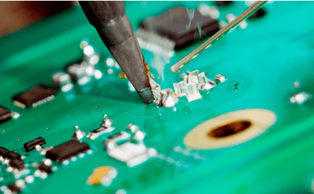
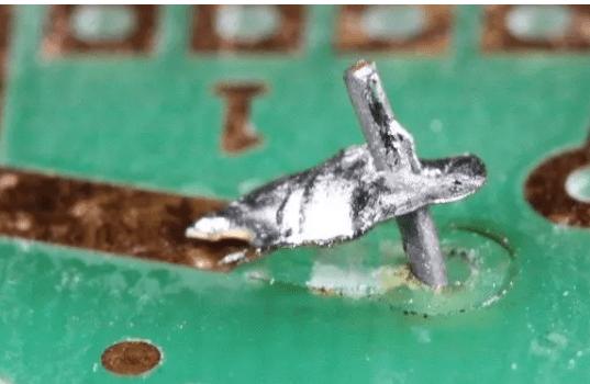
In the field of electronic repair and manufacturing, lifted PCB pads are a common yet frustrating problem. Many electronics enthusiasts are familiar with that moment of dismay when you carefully place a soldering iron on a circuit board, only to see the pad lift away with it.
Pad lifting typically occurs due to repeated soldering, excessive soldering heat, or physical stress, causing the copper foil to separate from the substrate. This situation is especially common during repairs and prototype development, but it doesn’t necessarily mean the board is scrapped.
Mastering pad repair techniques can not only salvage expensive circuit boards but also extend the lifespan of electronic products and reduce electronic waste. This article details various methods for repairing PCB pads, from simple to complex, to help you become a circuit board repair expert.
Understanding the Causes and Assessment of Lifted Pads
Before attempting to repair a pad, understanding the cause of the lifting and the extent of the damage is crucial. Pad lifting can generally be attributed to several common causes.
Overheating during soldering is the most common culprit. When the soldering iron temperature is too high or it remains on the same pad for too long, the adhesive between the copper foil and the substrate fails, causing the pad to lift or detach completely.
Multiple rework cycles also significantly increase the risk of pad lifting. Each repeated heating further weakens the bond between the pad and the PCB substrate.
Mechanical stress should not be overlooked – for instance, using excessive force when inserting or removing components, or aggressive scraping while cleaning solder joints, can lead to physical damage of the pad.
When assessing the extent of pad damage, several aspects need careful inspection: Confirm whether it’s just the surface of the pad that has peeled off, or if the trace has broken as well; Check if nearby components and traces are affected; Observe whether it’s a single-sided or multi-layer board, as this is crucial for selecting the appropriate repair method.
Identifying Damaged Pads
Before undertaking any repair or rework activity, it is necessary to identify the problem and its extent of damage. This provides a clear understanding of the defect and paves the way for the appropriate solution. Detecting damaged pads is critical and requires sufficient expertise. To understand how to repair a PCB pad, a careful visual inspection helps identify the main issues within the PCB, and this applies to damaged pads as well.
For compact and mixed PCBs, using a magnifying glass is recommended to carefully observe the fine details of the PCB. The next step is to perform electrical and continuity tests to find PCB defects, broken connections, or to determine if a pad is damaged based on various electrical parameters. In some cases, applying slight mechanical force to a component can also be helpful, as stress may cause the component to lift or shift, indicating improper or damaged pad connections.
Causes of Pad Damage
Numerous reasons, from the design to the manufacturing stage, can lead to pad damage. When designing a PCB, all potential factors leading to PCB pad failure should be considered. Here are some aspects that cause pad failure.
Design and Manufacturing Related Issues
PCB design is the first step before entering the manufacturing stage. All parameters and details are determined during the design phase and are further followed during manufacturing. Pad size, clearance, and orientation are all defined in the design stage. Any major or minor errors will inevitably lead to manufacturing errors in the pads. Even with an unreasonable pad design, issues like excessively thin copper foil thickness, insufficient bonding, low adhesion, and poor solder mask quality can lead to pad damage during the manufacturing stage. In such cases, knowing how to repair PCB pads helps engineers detect and correct design-related pad defects early.
Overheating
PTH and SMD components are soldered onto dedicated pads on the PCB. If the soldering iron temperature exceeds the specified value, prolonged heating can cause the pad to delaminate from the PCB and remove the copper. Overheating can also occur if the PCB has poor ventilation. Overheating may also damage inner layers and the solder mask. Understanding how to repair PCB pads is crucial for restoring adhesion and conductivity after thermal damage.
Mechanical Stress
PCBs are very sensitive to physical shocks; it is recommended to place them in a safe environment, free from external interference. Operations such as pulling out components, squeezing component leads, dragging components on the board, and mechanical impacts can tear or lift pads. Excessive stacking during storage and transportation can also damage PCB pads. In such mechanical failures, applying the correct technique to repair the PCB pad ensures structural restoration and maintains ongoing reliability.
Frequent Desoldering During Rework
Electronic components are soldered onto pads using standard assembly procedures. During PCB assembly and testing, certain components may need replacement. Regular desoldering weakens the pad strength; it is recommended to always operate carefully and correctly use flux, hot air, or controlled procedures. At this point, technicians often check how to repair PCB pads to maintain pad strength during multiple rework cycles.
Environmental Factors
Moisture, chemicals, and harsh environments often corrode copper pads. This degrades the performance of the solder mask and causes the copper to peel from the PCB. During PCB manufacturing, if cleaners and adhesives are not properly removed, deposited or contaminated substances can react with the copper, causing damage. For such environmental damage, learning how to repair PCB pads can prevent further corrosion and restore surface integrity.
Methods for Pad Repair
After identifying the problematic pads on the circuit board, we can determine which category of issue they belong to, and then proceed with the repair. Here are some commonly used methods for repairing pads.
Rewiring with Copper Wire (Bodge Wire/Jumper Wire)
For areas with less dense connections, using a bodge wire or jumper wire is the simplest and most direct repair method. This technique is particularly suitable for through-hole components and some surface-mount components.
Specific steps: First, scrape off the insulating lacquer from the copper foil at both ends of the breakpoint. Then, extract a few fine copper strands from a multi-strand copper wire, twist them together, and tin them. Solder the tinned wire end to the conductive copper foil, and wrap the other end around the component lead. Finally, trim the excess wire to complete the repair.
This method is simple and easy to implement but has limited strength and is suitable for areas not subject to significant stress.
Reballing/Resoldering a Damaged Pad
If the pad has minimal damage, low oxidation, slight cracks, or is partially lifted, re-soldering is more convenient. This method is simple and fast, requiring minimal resources. Clean the damaged pad with Isopropyl Alcohol (IPA) and remove residue. Apply flux and add new solder to cover the pad area. Then clean the pad again, add new solder, and test the continuity of the reworked pad. For minor surface damage, knowing how to repair a PCB pad allows for a quick fix without replacing the component.
Pad Replacement
If the pad is severely damaged, a holistic solution is more appropriate. Remove contaminants and clean the damaged pad on the PCB. Now, cut a copper strip or copper foil to the desired size, assembling it into a new pad. Align the pad orientation to the pad area and adhere it using adhesive or epoxy. Apply solder to the new pad for component connection. Now clean the board and test the circuit’s continuity. This technique requires extra work as the pad size must match the pad design. In cases of severe damage, the correct PCB pad repair method ensures the repaired pad matches the original electrical and mechanical properties.
Trace Repair
If the pad is completely damaged and the copper is also removed, the trace can be repaired using a jumper wire or a wire. While this method offers lower mechanical strength, it also carries the risk of poor connections. Use a thin wire to connect the trace of the missing pad, linking the missing trace. Solder the jumper wire to both ends of the trace, thereby ensuring circuit continuity. In complex rework situations, learning how to repair PCB pads helps technicians maintain conductivity and minimize rework errors.
PTH Pad Fixation
Pads for PTH components are larger in size and easier to repair. If the pad is lifted or almost impossible to remove, just a small amount of rework can restore the PCB to normal function. If the pad is missing, connection can also be restored by installing a suitable copper piece.
Preparations Before Repair
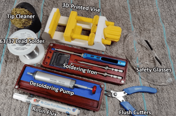
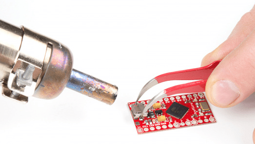
Successful repair begins with adequate preparation. The right tools and materials are the foundation of repair work, and a clean working environment can significantly improve the success rate.
Essential tools include: a temperature-controlled soldering iron (recommended power 30-60W, temperature controlled below 350°C), high-quality solder wire, flux, a multimeter, tweezers, a magnifying glass or microscope, a scraper or small knife.
Common materials include: thin copper wire (can be extracted from multi-strand wires), anhydrous alcohol or specialized PCB cleaner, UV-curable solder mask (green mask), and possibly replacement pads.
Cleaning the work area is an essential step. Thoroughly clean the soldering area with alcohol or a lint-free cloth to remove all oxides, grease, and flux residue. Ensure the area is completely dry before proceeding with the repair operation.
Safety precautions should not be neglected: Ensure you work in a well-ventilated area to avoid inhaling harmful fumes; Wear an anti-static wrist strap to prevent electrostatic discharge damage to sensitive components; Use appropriate eye protection.
Basic Repair Methods
Copper Wire Jumper Method
For areas with less dense connections, the copper wire jumper method is the simplest and most direct repair technique. This method is especially suitable for through-hole components and some surface-mount components.
Specific steps: First, scrape off the insulating coating from the copper foil at both ends of the broken trace. Then, extract several fine copper strands from a multi-strand wire, twist them together, and tin them. Solder the tinned end of the wire to the conductive copper foil, and wrap the other end around the component lead. Finally, trim any excess wire to complete the repair.
This method is simple and easy to execute but has limited mechanical strength, making it suitable for areas not subject to significant stress.
Utilizing an Adjacent Pad Method
When there is a spare pad or test point on the same net near the damaged pad, these points can be borrowed for connection.
Locate an adjacent pad connected to the lifted pad, ensuring the distance is not too far. After inserting the component lead into the pad hole (if applicable), bend the lead towards the borrowed pad. Solder the lead to the borrowed pad, taking care not to cause shorts with other pads. This method is quick and effective but requires the presence of suitable borrowing points on the circuit board.
Advanced Repair Techniques
Rebuilding Pads with Solder Mask (Green Mask) Method
For lifted surface-mount component pads, using solder mask (UV-curable resist) to rebuild the pad is a professional and reliable method.
First, thoroughly clean the damaged area with PCB cleaner. Use tweezers or a toothpick to carefully apply the solder mask, controlling its flow and shape. Expose the solder mask to UV light to cure it, determining the exposure time based on the product’s characteristics. After curing, use a precision knife to carefully scrape away the mask to expose the exact pad shape needed. Finally, tin the new pad and solder the component.
This method results in a repair close to the original but requires some skill and patience.
Pad Replacement Method
For completely detached pads, consider transplanting a same-sized pad from a scrapped circuit board for replacement.
Find a similar pad on a discarded PCB, removing it along with about 2mm of its connecting trace. Scrape off the oxide layer and residual solder mask from both sides of the connecting trace of the harvested pad, exposing the copper layer and tinning it. Use tweezers to hold the replacement pad in the lifted position, aligning the pad’s trace with the residual trace on the board so they overlap.
Solder the connection points of the traces with a soldering iron, then flatten the pad. Clean the area and apply a solder mask of the same color, followed by a curing process.
This method requires high technical skill but offers the most ideal repair outcome.
Repair of Special Pad Types

BGA Pad Repair
BGA pad repair is one of the most technically demanding operations in PCB repair. BGA pads can lift due to uneven heating or multiple rework cycles.
Professional repair methods include: Cleaning the repair area, removing the failed pad and a small section of its trace. Selecting a matching replacement pad; these specialized pads are typically made of copper foil, tin-plated on top, with an adhesive backing. Precisely position the new pad and bond it to the PCB surface using a hot press method. Then solder the new pad’s trace to the PCB circuit. Finally, apply a specialized resin to enhance bond strength.
This repair requires specialized tools and extensive experience, making it difficult for average hobbyists.
Repairing Inner Layer Damage in Multi-layer Boards
When pad lifting causes damage to the inner layer traces of a multi-layer board, the repair difficulty increases significantly. It is necessary to accurately determine the routing and connection relationships of the inner layer lines.
Use a multimeter to carefully measure and identify the inner layer traces that need connection. Drill a hole at an appropriate location to expose the inner layer copper foil that needs connecting. Use a thin copper wire passed through the hole to establish a connection with the inner layer trace, then route the wire to a suitable location on the surface. Finally, fill the drill hole with epoxy resin to secure the wire.
This repair is extremely delicate, requires professional equipment and rich experience. Sometimes, it might be more economical to consider replacing the circuit board altogether.
Post-Repair Inspection and Reinforcement
After completing the pad repair, comprehensive inspection and testing are essential to ensure repair quality and long-term reliability.
Electrical testing is the first step: Use a multimeter to check the connectivity of the repair point, ensuring there is no open circuit. Also, check for shorts between adjacent traces, especially in densely spaced areas. Perform a circuit function test to ensure the repaired circuit operates normally.
Mechanical reinforcement can enhance long-term reliability: Apply epoxy resin or specialized electronic glue around the connection points to enhance mechanical strength. For stress-prone areas, use hot melt adhesive to secure wires, reducing stress on the repair point.
For high-frequency or high-precision circuits, performance verification is also needed: Use an oscilloscope to check signal integrity, especially for high-frequency circuits. Measure voltages and currents at relevant points to ensure they meet design expectations. Perform appropriate aging tests to verify the reliability of the repair point under long-term use.
Methods to Prevent Pad Lifting
Prevention is better than cure. Taking appropriate preventive measures can significantly reduce the risk of pad lifting.
In terms of soldering technique: Control soldering iron temperature, avoiding excessively high temperatures (preferably below 350°C) and prolonged heating of the same joint. Use an appropriate amount of flux to improve solder flow and reduce heating time. Ensure the solder is completely molten before placing the component, avoiding applying excessive pressure.
Considerations for pad design: For pads requiring multiple soldering cycles, add teardrop pads at the design stage to strengthen the connection between the pad and the trace. Appropriately increase pad size, especially for connection points that need to withstand mechanical stress.
Rework: If multiple soldering cycles on the same pad are necessary, allow the pad to cool sufficiently between cycles. Consider using protective tape over vulnerable pads when soldering adjacent areas.
Best Practices for Pad Fixation
- Use similar solder, adhesives, flux, and cleaning materials to maintain the PCB’s original quality.
- During desoldering and resoldering, do not overheat the soldering iron tip. This could damage components surrounding the target area.
- Correct use of flux ensures smooth solder flow, improves wetting, and reduces oxidation.
- Properly mask new pads and apply a suitable surface coating at the end of the fixation process.
- Adequately test the PCB after rework to ensure the output is similar to before.
- Use appropriate workstations and standard procedures during repair activities.
Summary
Pads are essential on PCBs for connecting SMD components. These tiny parts often get damaged and require proper maintenance and fixation methods. Knowing how to repair PCB pads helps ensure reliable restoration when damage occurs and prevents further electrical issues. Handling these small, sensitive components requires the right tools, skills, experience, and processes.
If damaged PCB pads are properly repaired and the final product quality is maintained, the PCB can be used for a long time. However, it is always advisable to exercise caution during manufacturing, assembly, and usage to avoid the need for repair methods in the first place.


0 Comments