
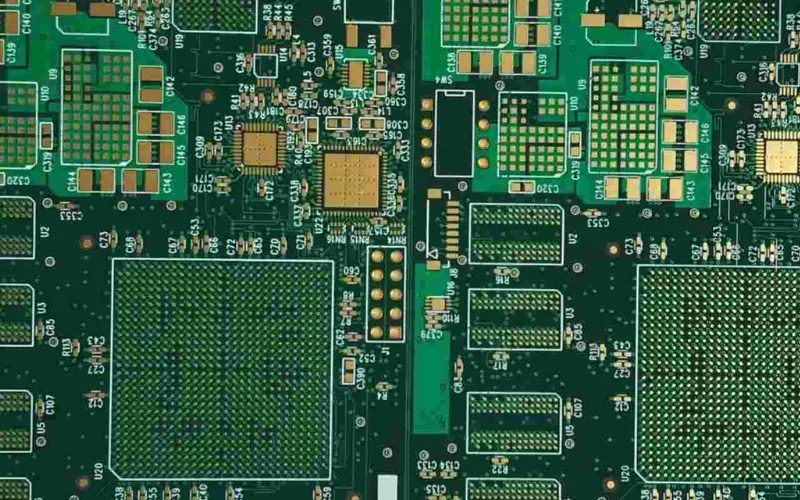
PCB thickness is important in design because it affects circuit conductivity, heat dissipation, mechanical strength, and signal integrity. Proper thickness ensures smooth electrical conduction, effective heat dissipation, and high reliability. Improper thickness selection can lead to problems such as signal attenuation, overheating, or connector mismatch.
Why is PCB thickness crucial in design?
PCB thickness not only impacts mechanical strength but also directly impacts signal integrity and electrical conductivity. Designers typically determine the appropriate thickness based on the PCB’s application, functional requirements, and assembly method. During production, PCB thickness is strictly controlled to ensure it meets design tolerances and performance requirements. Board thickness is tailored to the application. For example, high-power circuits require thicker copper layers and substrates to carry higher currents, while portable electronic devices tend to use thinner PCBs to reduce weight and save space.
Therefore, PCB thickness is more than just a dimensional parameter; it determines the board’s mechanical properties, signal transmission performance, and the current-carrying capacity of the copper traces. Most manufacturers adhere strictly to IPC standards when determining board thickness and tolerances for specific applications to ensure product reliability and consistency.
What is the thickness of 1.2mm PCB?
1.2mm refers to the total thickness of the entire PCB. This includes the total thickness of the substrate (such as FR4 fiberglass), copper foil, solder layer, solder mask, and other components. 1.2mm thick PCBs are a common option between thin and standard PCBs, offering both stability and flexibility. They are an ideal solution for designs requiring reliable electrical connections within limited space.
In practical applications, 1.2mm thick PCBs offer excellent mechanical strength and lightweight properties, making them a common medium-to-thin thickness suitable for electronic products with space and weight constraints. Examples include module circuit boards, LED driver boards, communication modules, and portable electronic devices.
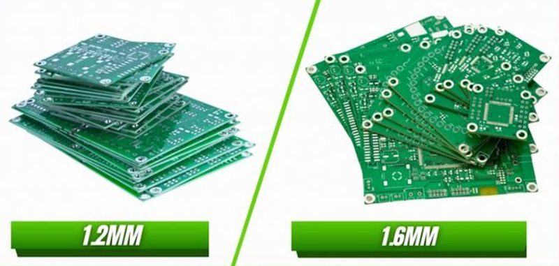
PCB thickness options: 1.2mm vs 1.6mm PCB
In PCB design, 1.2mm vs 1.6mm pcb are the two most common standard thicknesses. While the difference in appearance is only 0.4mm, there are significant differences in structural strength, thermal conductivity, and application scenarios. The choice of thickness often depends on product design requirements, space constraints, and electrical performance requirements.

Features of 1.2mm PCBs
Thinner thickness makes them suitable for compact devices: commonly used in modular circuits, wireless communication devices, LED driver boards, sensor modules, etc.
Lighter weight facilitates lightweight design in portable products;
Shorter thermal paths make them suitable for low- to medium-power applications;
Higher flexibility makes them suitable for devices requiring high vibration resistance.
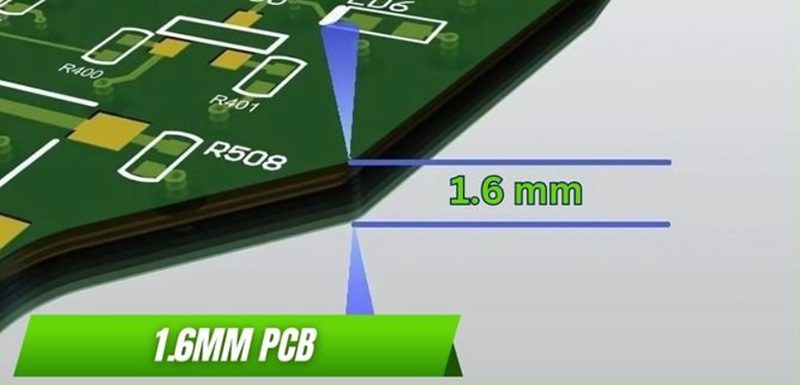
Features of 1.6mm PCBs
Industry standard thickness: 1.6mm is the most commonly used board thickness recommended by the IPC (Institute Connecting Electronics Industries) standard.
Strong structural stability: Suitable for multi-layer boards, high-speed signal boards, or high-power circuits;
Improved current carrying capacity: Suitable for high-current, high-power electronic components;
More balanced heat dissipation: Better for designs with demanding thermal management requirements.
There’s no absolute superiority or inferiority between 1.2mm vs 1.6mm pcb thicknesses; the choice depends on the product size, required strength, power load, and heat dissipation requirements. For those seeking thinness and flexibility, 1.2mm offers advantages; for stability and durability, 1.6mm is a more reliable option.
Is it better to have thinner PCB?
In PCB design, thinner is not always better. While thinner PCB offer advantages like lightweighting and space savings, they can also introduce a range of potential performance and reliability issues. The following analyzes the potential impacts of thin boards from several perspectives:
1. Reduced Mechanical Strength
The mechanical strength of a PCB is closely related to its thickness. Electronic products experience stresses such as vibration, impact, and bending during assembly, transportation, and long-term use. If a PCB is too thin, its bending resistance and overall rigidity will be significantly reduced, making it more susceptible to breakage, delamination, or solder joint cracking, leading to circuit failure. This is particularly noticeable in devices that require frequent plugging and unplugging or are subject to mechanical loads.
2. Limited Heat Dissipation
Modern electronic products typically feature a high level of integration and device density, which increases heat generation. PCB not only serve as a carrier for electrical connections but also serve as a heat conductor and dissipator. Thinner PCB have lower thermal capacity and shorter heat conduction paths, which can easily lead to localized overheating or heat accumulation, impacting component life and system stability. Conversely, a moderately thicker PCB can improve thermal conductivity and heat dissipation uniformity to a certain extent.
3. Reduced Current-Carrying Capacity
The copper foil layer in a PCB is responsible for current transmission and distribution, and current-carrying capacity is related to both copper and board thickness. Thinner PCBs typically mean closer conductor spacing and limited copper thickness, resulting in a reduced ability to carry high currents. In high-power or high-current applications, excessively thin PCBs can lead to current overload, copper trace overheating, and even burnout.
While thinner PCBs save space and weight, making them suitable for portable devices or flexible electronics, in most applications, excessively thin PCBs compromise mechanical strength, heat dissipation, and electrical reliability.
How to choose the right PCB thickness?
In PCB design, thickness not only affects mechanical strength and thermal conductivity but also directly impacts signal integrity, production processes, and product reliability. The following factors generally influence PCB thickness selection:
Copper Thickness
Copper layer thickness depends on the current the PCB needs to carry. Higher currents require thicker copper layers to ensure good conductivity and heat dissipation. However, thicker copper layers increase manufacturing costs due to increased material consumption and processing difficulty.

Substrate Material
The substrate material of a PCB is a key component in determining its performance. The choice of substrate depends on the product’s dielectric constant (Dk), glass transition temperature, and mechanical strength requirements.
Number of Layers
The more layers a circuit board has, the greater its overall thickness. Common 2- to 6-layer PCBs generally fall within the standard thickness range, while multilayer boards with 8 or more layers exceed the standard. When designing, avoid blindly pursuing thinner thickness to maintain form factor, as this may compromise electrical performance and structural stability.
Signal Type
Different signal types have different thickness requirements. For example, high-power signals require thicker copper layers and wider traces to reduce resistance and improve heat dissipation; high-speed signal circuits require stable dielectric thickness to ensure signal transmission integrity and impedance matching.

Via Type
The type of vias in a PCB (including through-holes, blind vias, buried vias, microvias, and via-in-pad) also affects the overall thickness. High-density interconnect (HDI) designs often require thinner laminates and microvia structures to save space and increase routing density.
Operating Environment
The operating environment of a PCB directly influences the thickness selection. Thinner PCBs may not remain stable in environments with high temperature, high humidity, or high vibration, while thicker PCBs offer advantages in mechanical strength and thermal stability. For applications carrying high current or power, thicker copper is recommended to enhance heat dissipation and reliability.

What to Consider When Choosing PCB Thickness?
Choosing the appropriate PCB thickness isn’t a simple parameter decision; it requires comprehensive consideration of multiple factors, including electrical performance, mechanical strength, heat dissipation efficiency, manufacturing processes, and assembly requirements. Choosing the right thickness can significantly improve product reliability and manufacturability.
Different application scenarios have varying requirements for PCB thickness. Consumer electronics (such as mobile phones and tablets) tend to use PCBs 1.0mm or thinner to save space and reduce weight. Industrial control, automotive electronics, or power supply products prioritize strength and heat resistance, typically opting for PCBs 1.6mm or thicker to ensure long-term stability and vibration resistance.
PCB thickness and copper layer thickness directly determine its current-carrying capacity and heat dissipation performance. High-power or high-current circuits require thicker substrates and copper foil to reduce conductor resistance and heat generation. Low-power signal circuits, on the other hand, can choose thinner PCBs to reduce cost and weight.
During the lamination, drilling, copper plating, and surface treatment processes, process parameters must be tailored to the board thickness. PCBs that are too thick or too thin increase manufacturing difficulty and cost. For example, a PCB that is too thin is prone to warping, while a board that is too thick can lead to problems such as drilling difficulties and inter-layer alignment deviation. Therefore, designers need to fully communicate with PCB manufacturers to determine the optimal thickness solution based on product applications and signal requirements to ensure that circuit performance fully meets production needs.
What is the optimal thickness of a PCB?
Standard PCB thicknesses fall within the following ranges: 0.78mm, 1.57mm, and 2.36mm, with 1.57mm being the most commonly used. User purchase quantity and application also determine the standard PCB thickness. From plywood as a substrate to epoxy resin today, substrate upgrades have also dictated thickness changes.
If your product requires a customized PCB thickness, we offer a variety of custom options designed to meet your specifications and needs. You can choose from designs with thicknesses ranging from 0.2mm to 6.3mm. You can also consult us for detailed information on factors to consider when selecting custom PCBs.
Is PCB thickness related to number of layers?
The number of layers in a circuit board (e.g., 2, 4, 6, or more) not only determines the complexity of signal routing but also directly impacts the overall thickness of the PCB. Each additional conductive layer (copper layer) requires corresponding dielectric and adhesive layers for isolation and connection, which increases the board thickness. As the number of PCB layers increases, the following factors contribute to thickness changes:
Increased stackup complexity: Each additional signal layer requires an additional dielectric and adhesive layer, increasing the overall thickness.
Increased conductor density: Multilayer boards require more routing space and power/ground planes to maintain signal integrity and electromagnetic compatibility, which indirectly increases thickness.
Mechanical strength requirements: High-layer boards are typically used in applications with higher structural strength requirements, such as industrial equipment, servers, and communications systems, and therefore tend to be thicker.
Overall, the key differences between 1.2mm vs 1.6mm pcb lie not only in thickness but also in the number of layers they support, structural stability, and application requirements. In actual projects, engineers typically select the most appropriate thickness based on product size, current load, thermal management, and assembly requirements to achieve the optimal balance between performance and structure.


0 Comments