




I once worked on a 10 Gbps backboard design that passed every simulation with comfortable margin. Signal integrity looked great. Impedance was controlled. Return loss was within spec. Then the prototype came back, and the eye diagram was a mess. The signals that were supposed to be clean and open at the receiver looked like someone had crumpled them up and tossed them into a trash can.
After three days of debugging with a VNA, the culprit turned out to be crosstalk. Not from some exotic coupling mechanism or a mystery source. Just two sets of high-speed differential pairs running side by side for about four inches on an inner layer. They were spaced at what we thought was a safe distance. It was not.
That experience taught me something that no textbook had made visceral enough: crosstalk is the silent saboteur of high-speed PCB design. It does not announce itself during schematic review. It does not always show up in basic impedance simulations. It creeps in during layout, hides in your stackup, and then reveals itself on the test bench when it is expensive and time-consuming to fix.
This article is the guide I wish I had back then. We will cover what crosstalk actually is, why it gets worse as signal speeds climb, the two distinct types you need to understand, the physical factors that control it, and most importantly, the practical techniques that actually work to reduce it in real PCB layouts.
What Is Crosstalk in PCB Design?
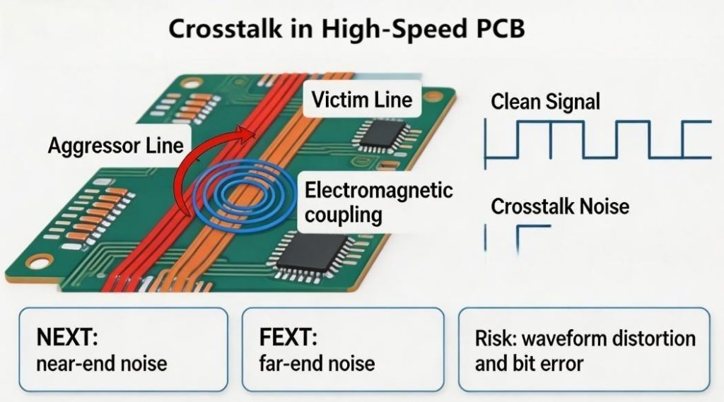
Crosstalk is the unwanted transfer of energy from one signal trace to an adjacent trace through electromagnetic coupling. In a high-speed PCB, every trace carries a signal that generates electric and magnetic fields. When another trace runs close enough to sit inside those fields, some of that energy gets coupled onto the second trace, appearing as noise.
The trace carrying the original signal is called the aggressor. The trace receiving the unwanted noise is called the victim. In most real-world situations, every trace is both an aggressor and a victim simultaneously, coupling noise onto its neighbors while receiving noise from them.
This matters because the noise injected by crosstalk adds to the signal on the victim trace. It distorts the waveform, reduces the noise margin, and in severe cases, causes the receiver to misinterpret a logic level. At low speeds, crosstalk is usually a minor nuisance that stays well below the noise threshold. At speeds above a few gigabits per second, the faster edge rates and higher frequencies make coupling much stronger, and crosstalk becomes one of the dominant signal integrity concerns.
A useful analogy: imagine two garden hoses lying side by side. If you pressurize one hose, the rubber wall bulges slightly. If the second hose is touching or very close, the deformation of the first hose can mechanically couple a pressure pulse into the second one. You did not connect the hoses, but energy transferred between them anyway. Crosstalk works the same way, except the coupling happens through electric and magnetic fields instead of mechanical pressure.
The Two Types of Crosstalk: NEXT and FEXT
Not all crosstalk behaves the same way. Engineers distinguish between two types based on where the noise appears relative to the signal source. Understanding the difference between near-end crosstalk and far-end crosstalk is essential, because they have different physical origins, different relationships to board geometry, and different mitigation strategies.
Near-End Crosstalk (NEXT)
Near-end crosstalk is the noise that appears on the victim trace at the end closest to the aggressor’s signal source. When the aggressor drives a signal into its trace, the coupling mechanisms inject energy into the victim trace in both directions. The portion that travels back toward the victim driver (the near end) is NEXT.
NEXT is produced by the combined effect of capacitive coupling and inductive coupling. Both mechanisms push energy in the backward direction along the victim trace, so they add together. This is why NEXT tends to be the stronger of the two crosstalk types in most PCB configurations.
One important characteristic of NEXT is that it saturates with coupling length. Once the coupled section of the traces exceeds a certain length (roughly related to the signal’s rise time and propagation velocity), the NEXT amplitude reaches a maximum value and stays there. Making the parallel run longer does not increase the peak NEXT voltage. This saturation behavior means that NEXT is primarily controlled by the coupling coefficient (which depends on spacing, dielectric height, and trace geometry) rather than by the length of the parallel run.
Far-End Crosstalk (FEXT)
Far-end crosstalk is the noise that appears on the victim trace at the end farthest from the aggressor’s signal source, the end where the victim’s receiver sits. This is the noise that directly threatens your signal margin at the receiver, which is why FEXT often gets more attention in high-speed design reviews.
FEXT is produced by the difference between capacitive and inductive coupling. Unlike NEXT, where both mechanisms reinforce each other, FEXT arises because capacitive and inductive coupling deliver energy in opposite directions along the victim trace. The net FEXT is proportional to the difference between the two coupling coefficients. In a symmetric stripline environment where the dielectric is uniform above and below the trace, this difference is theoretically zero. In a microstrip environment where the trace has air on one side and dielectric on the other, the difference is nonzero, and FEXT becomes a real concern.
The critical characteristic of FEXT is that it does not saturate. Instead, FEXT amplitude grows linearly with the coupled length. Every additional inch of parallel routing adds more far-end crosstalk. This is why long parallel runs of microstrip traces are particularly dangerous in high-speed designs, and why engineers go to considerable lengths to minimize the coupling length in microstrip routing.
NEXT vs. FEXT: Key Differences at a Glance
| Aspect | NEXT | FEXT |
|---|---|---|
| Where noise appears | Victim end near the source | Victim end far from the source |
| Coupling mechanism | Capacitive and inductive coupling add together | Capacitive and inductive coupling partially cancel |
| Effect of coupling length | Saturates after a critical length | Grows linearly with length |
| Stripline behavior | Still present, depends on spacing | Theoretically zero in symmetric stripline |
| Microstrip behavior | Present, typically larger than FEXT | Present and grows with length |
| Primary design lever | Increase spacing to reduce coupling coefficient | Reduce coupling length and prefer stripline routing |
What Causes Crosstalk in High-Speed PCBs?
Understanding the root causes of crosstalk requires looking at the electromagnetic coupling between traces and the board geometry that controls it.
Electromagnetic Coupling Mechanisms
When a signal travels along a trace, it creates two types of electromagnetic fields.
Capacitive coupling occurs through the electric field. The aggressor trace has a time-varying voltage that creates an electric field in the surrounding dielectric. If the victim trace is nearby, this field induces a current in the victim through the mutual capacitance between the two traces. The induced current flows in both directions along the victim, splitting between the near end and the far end.
Inductive coupling occurs through the magnetic field. The time-varying current in the aggressor creates a magnetic field that links with the victim trace, inducing a voltage through the mutual inductance. The induced voltage drives current in a specific direction along the victim trace, determined by Lenz’s law.
The total crosstalk at any point on the victim trace is the superposition of capacitive and inductive contributions. Whether they add or cancel depends on the direction of signal travel and the type of crosstalk being measured.
Key Factors That Influence Crosstalk Magnitude
Several physical parameters control how much crosstalk you get. Some of these you can control directly through layout decisions. Others are constrained by your stackup, manufacturing capabilities, or signal requirements.
Trace spacing is the most direct lever. The electromagnetic field strength drops rapidly with distance. Doubling the edge-to-edge spacing between two traces can reduce the coupling coefficient by 6 dB or more. This is why spacing rules exist and why they matter more at higher speeds.
Coupling length determines how much energy gets transferred. Longer parallel runs mean more opportunity for the fields to interact. For FEXT, the relationship is linear. For NEXT, it saturates, but only after a length that may still be substantial in a given design.
Signal edge rate is arguably the most critical factor from a system perspective. Crosstalk is driven by the rate of change of the aggressor signal, not by its frequency content in the traditional sense. A 2.5 Gbps signal with a 100 picosecond rise time produces more crosstalk than a 5 Gbps signal with a 300 picosecond rise time, even though the second signal has higher fundamental frequency. Faster edges couple more energy into adjacent traces.
Dielectric height to reference plane controls how tightly the field is confined to the trace. A trace sitting close to its reference plane has fields that are tightly bound and do not extend as far laterally. A trace far from its reference plane has fields that spread out more, increasing coupling to adjacent traces. This is one reason why thin dielectric layers in the signal routing layers help reduce crosstalk.
Dielectric constant affects the propagation velocity and the wavelength of the signals, but its direct effect on coupling coefficient is secondary compared to spacing and dielectric height.
Impedance discontinuities at vias, layer transitions, or width changes create reflections that can compound with crosstalk effects. A reflected signal can become an additional aggressor, coupling into yet another trace.
Via stubs on layer transitions act as small antennas at high frequencies. The stub resonance can inject broadband noise that couples into adjacent vias and traces, contributing to what appears as crosstalk but actually originates from the via structure.
How to Reduce Crosstalk in High-Speed PCB Design
This is the section that earns its keep on the design bench. Every technique below is something you can apply during layout to meaningfully reduce crosstalk in your high-speed boards.
Increase Trace Spacing
The single most effective way to reduce crosstalk is to put more distance between traces. The electromagnetic coupling between two parallel traces decreases as the spacing increases, and the relationship is strong enough that even small increases in spacing can yield significant improvements.
The 3W rule is the most commonly cited guideline. It states that the edge-to-edge spacing between adjacent signal traces should be at least three times the trace width. For example, if your trace width is 5 mils, the minimum spacing would be 15 mils. This rule provides a reasonable starting point for general-purpose designs and keeps the coupling coefficient to a level where crosstalk is manageable for most signal speeds up to about 5 Gbps.
The 3W rule is a guideline, not a law. It does not account for the specific dielectric height, the number of aggressors, or the required crosstalk budget for your particular design. In many high-speed designs above 10 Gbps, 3W spacing is not enough. This is where the 5W rule comes in. Spacing traces five trace widths apart reduces crosstalk further and provides more margin. The tradeoff is routing density, which becomes tighter and may require additional layers.
In practice, you need to balance spacing against your routing constraints. The key insight is that you should apply the tightest spacing rules to your highest-speed nets and relax the rules for slower signals where crosstalk is less of a concern. Not every trace on your board needs 5W spacing. Allocate your routing budget intelligently.
One nuance that is often overlooked: the spacing between a trace and its nearest neighbor matters most, but the cumulative effect of multiple aggressors on a single victim also matters. A victim trace sandwiched between two aggressors receives noise from both sides. If the aggressors are switching in opposite directions, their coupling effects partially cancel. If they are switching in the same direction, the effects add. Worst-case analysis should assume all aggressors are switching simultaneously in the worst-case direction.
Optimize Your Layer Stackup
The stackup is the foundation of your crosstalk performance, and it is one of the decisions that is hardest to change after the board is fabricated.
Stripline versus microstrip routing is one of the most consequential choices. In a stripline configuration, the signal trace is sandwiched between two reference planes with uniform dielectric above and below. The electromagnetic fields are well confined, and the symmetry of the structure causes the capacitive and inductive coupling components to produce zero far-end crosstalk in theory. NEXT is still present but is manageable with proper spacing.
In a microstrip configuration, the signal trace sits on the surface with a reference plane below and air above. The asymmetry means FEXT is nonzero and grows with coupling length. Microstrip is sometimes necessary for component placement on outer layers, but for your highest-speed signals, stripline routing on inner layers is strongly preferred.
Tight coupling to the reference plane means keeping the dielectric thickness between the signal layer and its reference plane as thin as practical. Thinner dielectric confines the fields more tightly around the trace, reducing the lateral extent of the field and therefore reducing coupling to adjacent traces. A typical high-speed stackup might use 3 to 4 mil dielectric thickness for signal layers, compared to 8 to 10 mil for lower-speed designs.
A well-designed high-speed stackup places signal layers on inner layers in stripline configuration, with thin dielectric to the reference planes, and reserves the outer layers for lower-speed signals or component pads. Each signal layer should have a continuous reference plane directly above or below it, ideally both. Return current path discontinuities caused by missing or split reference planes create additional coupling paths that worsen crosstalk.
Use Ground Guard Traces, But Do It Correctly
Guard traces are copper traces placed between two signal traces and connected to ground, intended to shield the victim from the aggressor by intercepting the coupling fields. The concept sounds logical, and guard traces do appear in many design guidelines.
The reality is more nuanced. A guard trace that is not properly grounded through a series of via connections to the reference plane does very little to reduce crosstalk. An unconnected or poorly connected guard trace can actually act as a resonant structure that redistributes coupling in unpredictable ways. Some studies and simulation results show that an ungrounded guard trace provides negligible improvement or even increases coupling at certain frequencies.
If you choose to use guard traces, ground them with vias at regular intervals along their length, spaced at no more than one-tenth of the wavelength at your highest frequency of interest. For a 10 Gbps signal, this means vias every few hundred mils. The guard trace must also be connected to the reference plane at both ends.
Even with proper via grounding, guard traces consume routing space that could alternatively be used to increase the spacing between signal traces. In many cases, taking the same copper area that a guard trace occupies and using it to widen the spacing between the aggressor and victim produces a greater crosstalk reduction than adding a guard trace between them. Consider guard traces as a secondary measure, not a primary one.
Control Impedance Continuity
Every impedance discontinuity on a trace creates a reflection. Reflected signals propagate along the trace and can couple onto adjacent traces as secondary crosstalk. Maintaining consistent trace width, consistent reference plane geometry, and consistent dielectric thickness along the entire signal path minimizes these reflections and their downstream crosstalk contribution.
This means paying attention to trace width transitions at layer changes, avoiding trace routing over gaps or splits in the reference plane, and ensuring that the impedance profile is smooth through vias and connectors. For differential pairs, it also means maintaining consistent intra-pair spacing and consistent spacing to adjacent pairs along the route.
Minimize Coupling Length
Since FEXT grows linearly with the length of the parallel run, reducing the distance over which two high-speed traces run parallel is one of the most effective FEXT reduction strategies.
In practice, this means avoiding long parallel runs of high-speed traces on the same layer. If two differential pairs need to travel the same general direction, consider staggering their routing so they overlap for only a short segment, or route them on different layers where the dielectric provides some vertical separation.
When long parallel runs are unavoidable, as they sometimes are in dense backplane or connector routing, the mitigation strategy shifts to increasing spacing and relying on stripline routing to suppress FEXT.
Reduce Rise Time Where Possible
The aggressor signal is the driver of crosstalk, and its edge rate determines how much energy couples into adjacent traces. If your timing budget allows a slower edge rate, using it directly reduces crosstalk without any layout changes.
Many modern FPGAs and high-speed transceivers allow you to configure the output driver slew rate. In designs where the signal path is short and the timing margin is generous, selecting a slower slew rate can significantly reduce crosstalk while maintaining timing compliance. This is a system-level decision that should be made in coordination with your SI analysis, but it is worth considering early in the design process.
Use Differential Pair Routing
Differential signaling provides inherent noise rejection that single-ended signaling does not. When a differential pair is properly routed with tight intra-pair spacing and symmetric geometry, common-mode noise (including coupled crosstalk) is rejected by the differential receiver. The receiver responds only to the voltage difference between the two traces, and noise that couples equally onto both traces appears as common-mode voltage that gets rejected.
This does not make differential pairs immune to crosstalk. If the coupling is asymmetric, or if the differential pair is poorly routed with length skew or impedance imbalance, crosstalk can convert from common-mode to differential-mode and appear in the received signal. Proper differential pair routing with matched lengths, consistent spacing, and symmetric reference planes is essential to realize the common-mode rejection benefit.
For inter-pair crosstalk (coupling between two different differential pairs), the spacing rules apply just as they do for single-ended traces. Differential pairs do not provide protection against coupling from adjacent pairs; they only provide protection against common-mode noise coupled onto both traces of the same pair.
Back-Drill Via Stubs
When a signal transitions between layers through a via, the portion of the via barrel that extends beyond the last connected layer is called a stub. This stub acts as an unterminated transmission line segment that resonates at frequencies related to its length. At and above the resonant frequency, the stub couples energy into the via and into adjacent structures, contributing to both insertion loss and crosstalk.
Back-drilling is a manufacturing process that removes the unused portion of the via barrel after lamination. By eliminating the stub, you remove the resonant structure and its associated coupling. For designs operating above 5 Gbps, back-drilling is often specified for critical signal vias. Above 10 Gbps, it is frequently mandatory.
The alternative to back-drilling is using blind or buried vias to avoid stubs entirely. These controlled-depth or layer-specific via structures are more expensive to fabricate but eliminate the stub problem without the additional back-drill process step.
Apply Proper Termination
Improperly terminated signal lines produce reflections that travel back and forth along the trace. These reflections can couple onto adjacent traces, creating what appears to be crosstalk but is actually reflection-induced noise from an impedance mismatch. Ensuring that every high-speed signal line is properly terminated at the source, destination, or both reduces the reflected energy available to couple into neighboring traces.
The choice of termination scheme (series, parallel, Thevenin, or AC termination) depends on the signaling standard and topology. What matters for crosstalk reduction is that the termination is effective at minimizing reflections across the frequency range of interest.
Crosstalk Simulation and Measurement
Designing by rules of thumb is a good start, but for high-speed designs running at 5 Gbps and above, you need to verify your crosstalk performance through simulation before fabrication and through measurement after fabrication.
When Do You Need Simulation?
If your signal speeds exceed 3 to 5 Gbps, or if your trace spacing is tighter than the 3W guideline, or if you are routing high-speed signals through a dense connector field where spacing constraints are severe, simulation is strongly recommended.
Common simulation tools for crosstalk analysis include:
HyperLynx SI from Siemens provides pre-layout and post-layout signal integrity simulation with built-in crosstalk analysis. It is widely used in the industry and integrates with popular PCB design tools.
Ansys SIwave is a full-wave solver that handles complex stackup geometries and provides S-parameter extraction including crosstalk terms. It is particularly useful for package and board-level analysis.
CST Studio Suite from Dassault Systemes provides 3D electromagnetic simulation capability for detailed analysis of vias, connectors, and other structures where analytical models break down.
Keysight ADS offers channel simulation and signal integrity analysis tools that can model crosstalk in the context of complete high-speed links including transmitter, channel, and receiver.
The simulation workflow typically starts with a stackup definition, followed by geometry extraction from your layout, and then S-parameter or time-domain simulation to extract crosstalk coefficients. You compare the results against your crosstalk budget to determine whether your design meets the requirements.
How to Measure Crosstalk in the Lab
After fabrication, you can measure crosstalk using a vector network analyzer (VNA) or through time-domain reflectometry (TDT) techniques.
A VNA measures the S-parameters of a multi-port network. For crosstalk characterization, you connect the aggressor port to port 1, the victim port to port 3 (near end) and port 4 (far end), and measure S31 (NEXT) and S41 (FEXT) as a function of frequency. The frequency-domain data can be converted to the time domain through inverse Fourier transform to see the crosstalk pulse shape and amplitude.
TDT measurement involves launching a step or pulse into the aggressor and observing the coupled signal on the victim using a high-bandwidth oscilloscope. This gives you a direct time-domain view of the crosstalk waveform, which is intuitive to interpret and relates directly to the noise margin impact.
Practical measurement challenges include designing test fixtures with controlled impedance, minimizing fixture crosstalk that could mask the board crosstalk, and calibrating the measurement system to remove the effects of connectors and cables. For multi-gigabit measurements, even the test fixture design requires careful SI analysis.
Interpreting Simulation and Measurement Results
The output of a crosstalk analysis is typically expressed as a peak noise voltage on the victim trace, either in the time domain or as a coupling coefficient in the frequency domain. The key question is whether this noise is acceptable.
A common guideline is that the total crosstalk noise on any victim trace should not exceed 5 to 10 percent of the signal swing. For a 1-volt differential signal, this means the crosstalk-induced noise should stay below 50 to 100 millivolts. For more aggressive designs with tighter noise margins, the budget may be even tighter.
When evaluating results, consider the worst case: all aggressors switching simultaneously in the same direction, maximum coupling length, and fastest edge rate. This worst case may be unlikely in real operation, but your design should have margin to handle it.
Practical Design Checklist: Reducing Crosstalk in Your Next High-Speed Board
Use this checklist during your layout review to catch crosstalk issues before fabrication.
- Identify all nets operating above 3 Gbps and flag them as high-speed for special spacing treatment.
- Apply minimum 3W spacing between high-speed traces. Increase to 5W or greater for signals above 10 Gbps.
- Route highest-speed signals on inner layers in stripline configuration whenever possible.
- Ensure every signal routing layer has a continuous reference plane directly above or below.
- Keep dielectric thickness between signal layers and reference planes at 4 mil or less for high-speed layers.
- Minimize the parallel coupling length between any two high-speed traces. Stagger routing if needed.
- If using guard traces, connect them to ground via with vias every 200 mils or less and terminate both ends.
- Verify that no high-speed trace crosses a split or gap in its reference plane.
- Back-drill via stubs on all signal vias connecting to layers above the last used layer for signals above 5 Gbps.
- Check intra-pair skew on all differential pairs. Keep skew below 5 mils for signals above 10 Gbps.
- Verify termination is applied on all high-speed point-to-point links.
- Run post-layout SI simulation including crosstalk analysis for all nets above 5 Gbps.
- Review crosstalk results against the crosstalk budget: total victim noise below 5 to 10 percent of signal swing.
- Document the crosstalk analysis results and stackup requirements for manufacturing.
Case Study: Diagnosing Crosstalk on a 10 Gbps Backplane
A few years ago, a client came to us with a backplane design that was failing compliance testing. The board was a 20-layer construction with multiple 10 Gbps differential pairs routed between connectors on the top and bottom. The design had passed basic impedance checks and basic insertion loss measurements were within spec. But the eye diagrams at the receivers were consistently degraded, with closure that could not be attributed to loss alone.
We started by extracting the stackup and performing post-layout SI simulation using the actual trace geometry from the gerber files. The simulation revealed that two groups of differential pairs shared an inner routing layer for approximately six inches, with edge-to-edge spacing of about 8 mils on 4 mil-wide traces. That is less than 2W spacing, far below the recommended guideline for 10 Gbps signals.
The simulation showed NEXT coupling coefficients of minus 30 dB and FEXT contributions that added up across the coupling length to produce peak noise voltages of about 60 millivolts on the victim pairs. Given the signal swing of 800 millivolts, that was roughly 7.5 percent crosstalk noise, right at the edge of the acceptable budget and enough to close the eye when combined with loss and jitter.
The fix involved three changes. First, we rerouted the most critical pairs to inner layers where they could have the routing layer to themselves with at least 5W spacing. Second, we adjusted the stackup on two layers to reduce the dielectric thickness from 5 mils to 3.5 mils, tightening the field confinement for pairs that could not be rerouted. Third, we added back-drilling to 14 vias on the highest-speed nets where stub lengths exceeded 10 mils.
After respin, the eye diagrams opened significantly. The crosstalk contribution dropped from 60 millivolts to under 20 millivolts, and the compliance test passed with margin. The total cost of the respin was significant, but it could have been avoided entirely if the crosstalk simulation had been part of the original design flow.
Frequently Asked Questions
What is crosstalk in a high-speed PCB?
Crosstalk is the unwanted electromagnetic coupling between adjacent signal traces on a PCB. When a signal on one trace (the aggressor) generates time-varying electric and magnetic fields, those fields can induce noise on a nearby trace (the victim). At high speeds, this noise can become large enough to cause signal integrity violations.
What is the difference between NEXT and FEXT?
Near-end crosstalk (NEXT) appears on the victim trace at the end closest to the aggressor signal source, while far-end crosstalk (FEXT) appears at the end farthest from the source. NEXT saturates with coupling length, while FEXT grows linearly with coupling length. In symmetric stripline, FEXT is theoretically zero, but it is significant in microstrip configurations.
Does the 3W rule really reduce crosstalk?
The 3W rule, which specifies edge-to-edge spacing of three times the trace width, provides a practical starting point for crosstalk reduction in designs up to about 5 Gbps. For higher-speed signals, especially above 10 Gbps, wider spacing such as 5W or more may be necessary. The 3W rule is a guideline, not a guarantee, and should be validated through simulation for critical nets.
How does trace spacing affect crosstalk?
Electromagnetic coupling strength decreases rapidly with increasing distance between traces. Doubling the edge-to-edge spacing can reduce the coupling coefficient by 6 dB or more. Spacing is the most direct and effective layout lever for controlling crosstalk.
Why is crosstalk worse in microstrip than stripline?
In microstrip, the signal trace has air on one side and dielectric on the other, creating an asymmetric field distribution. This asymmetry means the capacitive and inductive coupling contributions do not cancel for far-end crosstalk, so FEXT grows with coupling length. In symmetric stripline, the uniform dielectric environment causes the FEXT contributions to cancel, leaving NEXT as the primary concern.
Do ground guard traces reduce crosstalk?
Guard traces can reduce crosstalk, but only if they are properly grounded through a continuous series of via connections to the reference plane. Ungrounded or poorly grounded guard traces provide negligible benefit and can occasionally worsen coupling through resonance. In many cases, using the same copper area to increase spacing between signal traces provides more crosstalk reduction than adding a guard trace.
How do I simulate crosstalk before manufacturing?
Use a signal integrity simulation tool such as HyperLynx SI, Ansys SIwave, CST Studio, or Keysight ADS. Define your stackup, extract trace geometry from your layout, and run S-parameter or time-domain simulation to extract NEXT and FEXT coefficients. Compare the results against your crosstalk budget.
At what signal speed does crosstalk become a serious problem?
Crosstalk becomes a significant concern for most designs when signal edge rates drop below approximately 100 picoseconds, which typically corresponds to data rates above 3 to 5 Gbps. Above 10 Gbps, crosstalk is one of the dominant signal integrity challenges and must be addressed proactively in the design process.
Can via stubs cause crosstalk?
Yes. Via stubs resonate at frequencies determined by their length. At and above the resonant frequency, the stub couples energy into adjacent vias and traces, contributing to what appears as broadband crosstalk. Back-drilling removes unused via stubs and eliminates this coupling mechanism.
What is the acceptable crosstalk level for a high-speed design?
A widely used guideline is that total crosstalk noise on any victim trace should not exceed 5 to 10 percent of the signal swing. For tighter designs with reduced noise margins, the acceptable limit may be lower. The specific requirement depends on the signaling standard, receiver sensitivity, and overall noise budget.
Final Thoughts
Crosstalk is one of those problems that is easy to ignore during the early stages of design and painful to deal with after fabrication. The good news is that it is also one of the most controllable signal integrity challenges, provided you understand the physics and apply the right techniques during layout.
Spacing is your most powerful tool. Stackup optimization is your second. Simulation is your safety net. Together, these three elements form a practical framework for managing crosstalk in virtually any high-speed design.



0 Comments