



What Is PCB Desoldering and Why Is It Important?
PCB desoldering is the professional process of melting and removing solder joints, faulty components, and outdated electronic parts from printed circuit boards for repair, component replacement, and circuit rework. Learning how to desolder PCB safely and correctly is essential for electronics technicians, hardware designers, and maintenance engineers to avoid board scrapping and improve rework success rates. This practical skill applies to PCB prototype modification, defective component replacement, small-batch rework, and post-production repairs for all electronic circuit board projects.
Improper PCB desoldering techniques frequently cause common board damages, including lifted copper traces, cracked solder pads, substrate delamination, and burnt circuit layers. These avoidable errors render functional PCBs unusable, waste manufacturing resources, and delay project progress. Standardized, safe desoldering workflows ensure clean solder removal and reliable PCB rework for both through-hole and miniature SMD circuit board components.
What Tools Do You Need to Desolder PCB Successfully?
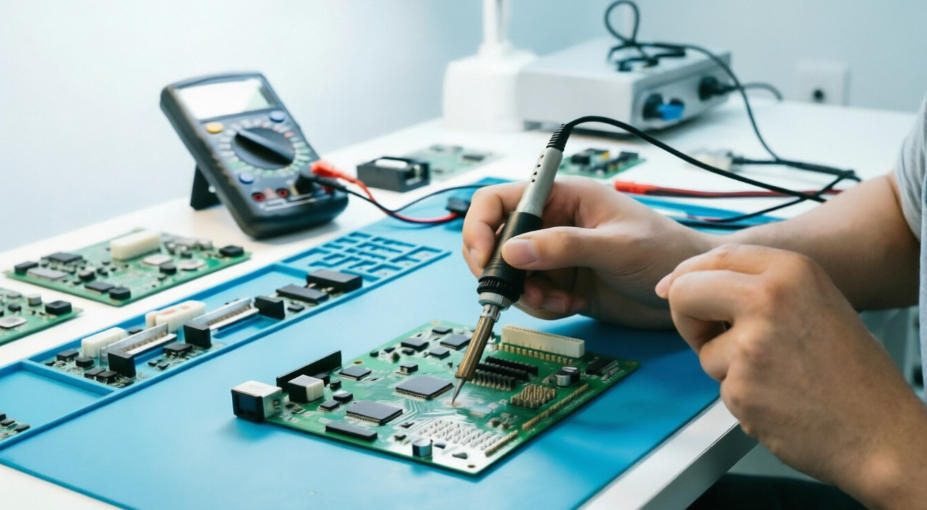
Safe and effective PCB desoldering relies on professional, well-matched desoldering tools and standardized operating procedures. Using specialized tools for different component types eliminates common beginner issues, such as incomplete solder removal, substrate burns, and lifted pads. Proper tool selection significantly boosts PCB rework efficiency and preserves original circuit board integrity during component desoldering.
| Desoldering Tool | Core Function | Best Usage Scenario |
| Temperature-Controlled Soldering Iron | Melts existing solder evenly without overheating the PCB substrate | All basic through-hole and small SMD desoldering tasks |
| Desoldering Pump (Solder Sucker) | Quickly vacuums large volumes of molten solder from pad holes | Clearing through-hole component leads and bulk solder buildup |
| Desoldering Braid (Solder Wick) | Absorbs thin residual solder from flat SMD pads | Fine cleaning for tiny surface-mount pads and joint gaps |
| No-Clean Flux | Enhances solder fluidity and prevents pad oxidation during heating | All desoldering processes, especially for aged or oxidized solder joints |
| Anti-Static Tweezers | Securely grips and lifts components to avoid static damage | Removing delicate SMD chips and small electronic parts |
| Hot Air Station | Delivers uniform heat for large multi-pin components | Desoldering ICs, connectors, and dense multi-pin modules |
How to Desolder Through-Hole PCB Components (Step-by-Step)
Through-hole PCB desoldering is the most fundamental and widely adopted circuit board rework method, featuring low operational difficulty and minimal board damage risks. This step-by-step guide explains how to safely desolder through-hole PCB components, fully clear solder from pin holes, and preserve intact pads and traces for component reinstallation and board repair.
Step 1: Preheat and Prepare the Joint
Set your soldering iron temperature between 315°C and 370°C. Apply a small amount of fresh flux to each through-hole solder joint to soften aged solder and improve fluidity.
Step 2: Melt and Remove Bulk Solder
Place the heated iron tip against the solder joint until the solder melts completely. Use a desoldering pump to fully vacuum molten solder out of the pin holes.
Step 3: Extract the Component
Gently wiggle the component leads while reheating any residual solder. Pull the component straight out once all pins are free from solder restraints.
Step 4: Clean Residual Solder
Use desoldering braid with mild heat to remove leftover solder from pad surfaces. Inspect pin holes to ensure no blockage remains before reinstallation.
How to Desolder SMD PCB Components Without Damaging Traces?
Precision SMD PCB desoldering is more complex than through-hole rework due to miniature surface-mount pads, dense circuit layouts, and fragile copper traces. Mastering proper heating and component lifting techniques allows you to desolder SMD PCB components cleanly without peeling pads or damaging high-density circuit structures.
Step 1: Apply Ample Flux
Cover all SMD solder joints with no-clean flux. Flux shortens heating time and protects pads from oxidation during repeated heat cycles.
Step 2: Uniform Heating
Use a hot air station at low to medium airflow to heat the entire component evenly. Avoid concentrated heat on individual pads to prevent localized overheating.
Step 3: Lift Components Gently
Once all solder joints melt simultaneously, use anti-static tweezers to lift the component vertically. Avoid twisting or tilting the part to prevent trace peeling.
Step 4: Level SMD Pads
Clean residual solder using desoldering braid. Keep pad surfaces flat and intact to ensure reliable soldering and stable electrical connections for new components.
What Are the Most Common PCB Desoldering Mistakes to Avoid?
Nearly all irreversible PCB damage during rework stems from incorrect desoldering practices rather than tool malfunctions. Recognizing these common PCB desoldering mistakes helps technicians avoid trace damage, pad loss, and substrate burnout, ensuring high-quality circuit board rework and long-term device stability.
- Overheating the substrate: Prolonged high heat burns FR-4 substrates and causes internal PCB layer delamination
- Forcible component removal: Aggressive twisting or lifting tears copper traces and destroys pad structures
- Skipping flux application: Dry solder requires excessive heating and leaves stubborn residual solder deposits
- Uneven multi-pin heating: Partial solder melting leads to bent pins and incomplete component removal
- Reusing contaminated tools: Oxidized iron tips deliver poor heat transfer and damage delicate pads
What Are Industrial PCB Desoldering Application Cases?
Professional PCB desoldering and precise circuit board rework are essential for mainstream electronics manufacturing and equipment maintenance. Different industries require tailored desoldering standards based on PCB precision grades, operating environments, and component types. Below are practical industrial PCB desoldering use cases covering four high-demand electronics fields.
1. Consumer Electronics
Smartphone and wearable device PCBs feature compact SMD layouts. Precision desoldering enables safe replacement of faulty charging ICs and sensor chips. This process resolves device failures caused by defective miniature components and extends product service life.
2. Automotive Electronics
Vehicle control PCBs and battery management PCBA units adhere to strict reliability standards. Standard desoldering procedures safely replace damaged resistors and capacitors. This practice avoids full board scrapping and sustains stable operation of automotive electronic systems.
3. Industrial Control & Automation
PLC and sensor module PCBs commonly suffer from component aging. Professional desoldering removes outdated or faulty industrial components effectively. It supports routine equipment maintenance and minimizes downtime for automated production lines.
4. Medical Electronics
Portable medical device PCBs require high precision and stability. Fine desoldering techniques replace faulty signal acquisition chips accurately. This maintains medical equipment measurement accuracy and complies with strict industry safety standards.
How to Fix Damaged Pads and Traces After Bad Desoldering?
Lifted pads, peeled traces, and residual solder damage are typical issues resulting from improper PCB desoldering. Most minor circuit board damages can be repaired through standardized professional rework procedures, fully restoring PCB electrical functionality and salvaging valuable prototype or mass-production circuit boards.
Simple Repair Workflow
- Clean damaged areas with isopropyl alcohol to remove residual flux and solder residue
- Use fine copper wire to rebuild broken trace connections
- Apply solder mask to insulate repaired areas and prevent short circuits
- Test circuit continuity to verify full electrical functionality
What Is the Difference Between Desoldering Braid vs Desoldering Pump?
Desoldering pumps and desoldering braids are the two primary tools for PCB solder removal, yet they serve entirely different desoldering scenarios. Using the wrong tool leads to incomplete solder cleaning and accidental PCB damage. This detailed comparison guides you to select the optimal tool for through-hole and SMD PCB desoldering tasks.
| Tool Type | Advantages | Limitations | Best Application |
| Desoldering Pump | Rapid bulk solder removal, ideal for efficient pin hole cleaning | Performs poorly on flat SMD pads and often leaves residual solder | Through-hole component desoldering and thorough pin hole cleaning |
| Desoldering Braid | Delicate residual solder cleaning with zero pad damage | Slow operation speed, unsuitable for large-scale solder removal | SMD pad polishing and fine residual solder removal |
FAQ: Frequently Asked Questions About PCB Desoldering
Most beginners and junior electronics technicians encounter similar challenges during daily PCB desoldering and circuit rework. These targeted FAQs answer the most frequently searched questions regarding safe PCB desoldering, tool operation, temperature control, and common troubleshooting issues for practical on-site reference.
1. Can you desolder PCB components without a soldering iron?
No. Heat is mandatory to melt solder and separate components from PCBs. While hot air stations can replace traditional soldering irons for large SMD components, non-thermal tools cannot remove solid solder joints safely or effectively.
2. Is lifted PCB pad repairable after desoldering?
Yes. Minor lifted pads can be repaired through trace jumping and fine copper wire rewiring. Severe pad peeling and substrate damage require professional board rework or full replacement.
3. What temperature is safest for PCB desoldering?
The safest temperature range for standard PCB desoldering is 315°C to 370°C. Temperatures below this range result in incomplete solder melting, while higher heat easily burns substrates and damages fragile copper traces.
4. Why does solder stay sticky after desoldering?
Sticky residual solder typically stems from insufficient flux application or inadequate heating temperatures. Applying fresh flux and reheating the joint thoroughly can eliminate all sticky solder residue.
Get Professional PCB & PCBA Solutions From Thindry
High-quality custom PCB and precision PCBA manufacturing greatly reduce desoldering and rework difficulty. Well-fabricated circuit boards feature uniform solder distribution, firm pad adhesion, and stable layer structures, effectively preventing pad lifting and trace damage during PCB desoldering procedures.
Thindry provides reliable one-stop PCB manufacturing and PCBA assembly services for global electronic engineers and enterprises. We support full on-demand customization for industrial, automotive, medical, and consumer electronic PCBs, and deliver a free DFM report for every project to eliminate structural defects and reduce subsequent desoldering rework risks.
If you have any PCB design, customization, prototyping, or mass production needs, contact our professional technical team for reliable support and order collaboration. You can reach us via email: sales@pcbtry.com.

0 Comments