




PCB layout is a core engineering process that converts abstract circuit schematics into physical, manufacturable printed circuit board structures. Learning and understanding what is PCB layout empowers hardware engineers, design teams, and supply chain professionals to build stable electronic circuits while avoiding common manufacturing and performance failures. This practical 2026 guide covers detailed PCB layout definitions, step-by-step PCB layout workflows, industry-standard design rules, real-world industrial PCB layout cases, common PCB layout mistakes, and professional optimization strategies to deliver actionable engineering value for beginners and professional designers alike.
What Exactly Is PCB Layout in Electronic Design?
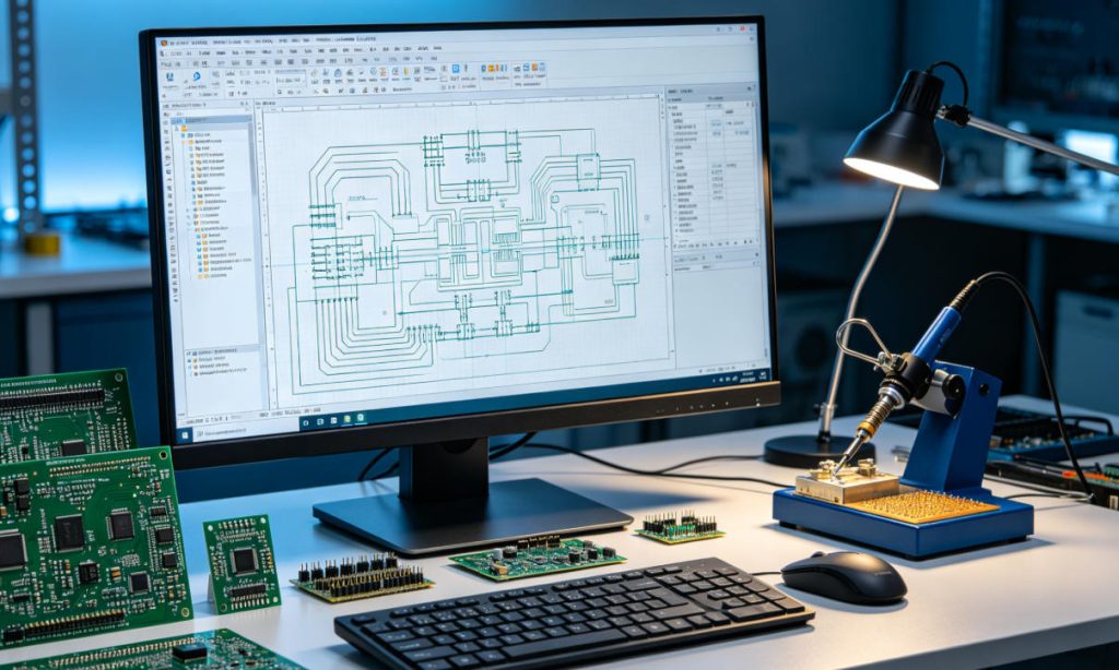
PCB layout describes the complete physical arrangement of electronic components, conductive traces, vias, and grounding structures on a printed circuit board. It acts as the critical bridge between theoretical schematic logic and real-world hardware implementation, defining the overall quality of every electronic circuit. Every layout decision directly defines a device’s electrical performance, stability, and manufacturability.
Core nature of PCB layout
Schematic design focuses purely on establishing logical circuit connection relationships, while professional PCB layout focuses entirely on scientific physical spatial arrangement of all board elements. Layout engineers define component positioning, trace paths, layer distribution, and via placement. This process turns virtual circuit logic into fully producible physical hardware.
Key responsibilities of PCB layout work
Complete PCB layout work includes modular component placement, precise signal routing, power and ground plane design, thermal optimization, and strict DFM compliance. Every layout detail impacts signal integrity, heat dissipation efficiency, production yield, and the long-term service life of electronic products.
What Is the Difference Between PCB Design and PCB Layout?
Many engineering professionals mistakenly treat PCB design and PCB layout as the same process, but they are separate, sequential engineering stages. PCB design covers high-level logical planning, while PCB layout executes physical circuit implementation. Each stage features unique workflows, core focuses, and technical objectives.
| Item | PCB Design | PCB Layout |
|---|---|---|
| Core Focus | Circuit logic, functional verification, schematic drawing | Physical placement, routing, manufacturability optimization |
| Work Stage | Early electronic product development | Mid-stage physical board implementation |
| Technical Goal | Ensure circuit functions meet design requirements | Ensure stable performance and smooth mass production |
| Tool Application | Schematic editing, circuit simulation tools | EDA layout tools, DFM detection tools |
What Are the Core Steps of Standard PCB Layout Workflow?
A standardized PCB layout workflow eliminates redundant revisions and ensures consistent design accuracy. This industry-proven process includes pre-layout preparation, modular physical design, and post-layout validation. It applies to all consumer, industrial, automotive, and medical PCB development projects.
Pre-layout preparation
Engineers must confirm board outline dimensions, component footprints, and functional project requirements before starting layout work. Full schematic verification eliminates logical errors upfront. This foundational step prevents major layout reworks in later design stages.
Component modular placement
Group all components by functional modules, including power supply, signal processing, and control circuits. Isolate heat-generating components from sensitive signal components to avoid electromagnetic interference. Always reserve standardized gaps for assembly and thermal dissipation.
Layer planning and routing
Plan single-layer, double-layer, or multi-layer stackups based on circuit complexity and signal speed. Complete power distribution routing, low-speed signal routing, and high-speed differential pair layout strictly per industry rules. Rational layer planning drastically improves circuit stability.
Grounding and thermal optimization
Implement dedicated ground planes for analog and digital circuit domains to reduce system noise. Optimize the placement of high-power components to eliminate localized overheating risks. Reliable grounding and thermal design greatly enhance overall circuit operational stability.
Post-layout DFM verification
Perform comprehensive DFM checks for trace width, clearance, via dimensions, and component spacing. Verify full manufacturability to resolve potential production obstacles before finalizing design files. This step guarantees high-yield mass production.
What Key Rules Must Professional PCB Layout Follow?
Professional PCB layout must comply with three core rule sets: electrical performance standards, structural assembly specifications, and manufacturing process guidelines. These standardized rules ensure stable circuit operation, high production yields, and long-term product reliability across all industries.
Electrical performance rules
Use 45-degree angle traces exclusively to prevent signal reflection caused by sharp right-angle turns. Maintain uniform trace spacing to suppress crosstalk between adjacent lines. Implement precise impedance matching for all high-speed signal pathways.
Manufacturing process rules
Set all trace widths, via diameters, and pad spacing parameters within standard manufacturing tolerances. Avoid ultra-miniature specifications that exceed conventional production capabilities. Consistent parameter settings ensure perfect design-to-production compatibility.
Structural and thermal rules
Reserve adequate assembly clearance and thermal dissipation space for all components. Physically isolate high-temperature power components from precision sensitive devices. This practice prevents signal degradation and permanent component damage.
What Are Common PCB Layout Mistakes That Ruin Product Performance?
Nearly all PCB performance failures stem from consistent layout errors made by new and intermediate designers. Most of these mistakes go unnoticed in software simulation. They only cause signal instability, thermal overload, or production scrapping in physical hardware testing.
Unreasonable component layout
Random mixing of analog and digital components or overcrowded heat-generating parts creates severe electromagnetic noise and poor thermal dissipation. This common layout mistake is the leading cause of unstable operation for precision electronic devices and sensor systems.
Non-standard trace routing
Extended parallel high-speed traces, untrimmed trace stubs, and mismatched differential pair lengths trigger signal attenuation and transmission errors. High-frequency communication and automotive circuits are extremely vulnerable to these non-standard routing defects.
Ignoring DFM design constraints
Excessively dense component layout, irregular via placement, and insufficient assembly gaps render PCBs unmanufacturable. Countless designs pass virtual simulation yet fail mass production due to overlooked DFM layout constraints.
How Does PCB Layout Affect Electronic Product Reliability?
Professional engineering data confirms that PCB layout directly controls roughly 60% of an electronic product’s stability and service lifespan. Strategic layout optimizes signal transmission, thermal management, and anti-interference performance. Poor layout creates latent failure risks and shortens product lifecycle drastically.
Influence on signal integrity
Standardized PCB layout guarantees clean, stable high-speed signal transmission and minimizes crosstalk and signal reflection. Poorly optimized layout causes frequent data loss and latency issues in communication systems and industrial control hardware.
Influence on thermal stability
Scientific thermal layout balances board temperature distribution and prevents premature component aging or burnout. Improper heat dissipation design leads to random device crashes during high-load and continuous operation scenarios.
Influence on production yield
DFM-compliant PCB layout effectively eliminates short circuits, open circuits, and soldering defects during manufacturing. It significantly improves mass production yield rates and reduces long-term after-sales failure rates for electronic products.
What Are Typical Industrial Application Cases of PCB Layout?
PCB layout design standards vary drastically across different industrial sectors. Each industry requires customized layout optimization to match unique working environments and certification requirements. Below are four high-demand industry cases with practical layout solutions.
Automotive Electronics PCB Layout
Automotive electronic PCB layout applies to vehicle ADAS sensors, powertrain control units, and in-vehicle infotainment systems. It solves extreme temperature fluctuation, mechanical vibration, and strong on-board electromagnetic interference. Layout strictly follows AEC-Q industry standards and modular signal isolation for driving safety.
Medical Electronics PCB Layout
Medical electronic PCB layout serves portable diagnostic tools, patient monitoring devices, and precision therapeutic equipment. It addresses strict low-noise and high-precision signal acquisition requirements. Layout isolates weak biological signal traces from power noise and complies with ISO 13485 medical certification norms.
Industrial Control PCB Layout
Industrial control PCB layout supports PLC controllers, data acquisition sensor modules, and automated manufacturing equipment. It resists severe on-site electromagnetic interference and enables 24/7 continuous operation. Layout uses thickened power traces and full grounding coverage for maximum stability.
Communication Equipment PCB Layout
Communication equipment PCB layout powers 5G communication modules, network routers, and base station signal transmission hardware. It stabilizes high-speed signal impedance and suppresses radio frequency interference. Precise differential pair control and impedance tuning ensure uninterrupted data communication.
What Is the Difference Between Beginner and Professional PCB Layout?
The core difference between beginner and professional PCB layout lies in multi-dimensional optimization capabilities. New designers focus only on basic circuit functionality. Professional engineers balance electrical performance, manufacturability, and long-term operational reliability.
Design thinking difference
Beginners only complete basic trace connection to achieve circuit functionality. Professional designers comprehensively optimize signal integrity, thermal dissipation, production feasibility, and future maintainability for every layout project.
Rule application difference
New layout designers lack standardized awareness and frequently ignore DFM and EMC design rules. Professional PCB layout strictly enforces industry-specific standards tailored to each product’s application scenario.
Problem-solving difference
Beginners can only finish fundamental layout tasks according to schematics. Professional proactively identifies and resolves hidden issues including crosstalk, thermal overheating, and impedance mismatch to enhance overall product stability.
How to Optimize PCB Layout for Better Signal Integrity?
Signal integrity optimization is the core of high-grade PCB layout design. Targeted layout adjustments effectively eliminate high-speed signal attenuation, crosstalk, and reflection errors. This optimization method is essential for precision and high-frequency electronic devices.
Optimize high-speed signal routing
Follow the standard 3W spacing rule for all high-speed signal traces. Maintain equal length and parallel alignment for differential pairs. Minimize unnecessary vias and trace stubs to preserve stable signal transmission quality.
Standardize grounding design
Implement separated analog and digital grounding with full ground plane coverage. Adopt single-point grounding techniques to suppress system-level noise. This method significantly improves the circuit’s anti-interference capability.
Precise impedance matching
Adjust trace width and PCB dielectric thickness based on specific signal frequency parameters. Accurate impedance matching eliminates signal reflection and power transmission loss. It greatly boosts high-speed circuit transmission efficiency and stability.
Why Is DFM Optimization Indispensable in PCB Layout?
DFM optimization is indispensable for reliable PCB layout design and mass production. Many high-performance layout designs fail commercialization due to unaddressed manufacturing rule conflicts. This causes project delays and unnecessary engineering resource waste.
Avoid manufacturing defects
Strict DFM optimization standardizes trace width, via dimension, and component spacing parameters. It effectively prevents short circuits, open circuits, and empty soldering defects during PCB manufacturing and assembly.
Improve production efficiency
Optimized DFM-friendly layout reduces overall manufacturing difficulty and simplifies SMT assembly workflows. It shortens prototype iteration cycles and accelerates mass production schedules for electronic enterprises.
Reduce project revision costs
Proactive DFM verification before final design delivery avoids repeated layout revisions caused by production failures. It stabilizes project progress and significantly improves overall engineering delivery efficiency.
Thindry supports on-demand customization and provides free DFM reports for all PCB and PCBA projects. Our professional engineering team verifies layout manufacturability in advance, eliminates potential design flaws, and ensures one-time successful mass production for all clients.
FAQ: Frequently Asked Questions About PCB Layout
These curated FAQs resolve the most common doubts about PCB layout from designers, technicians, and industry beginners. All answers deliver straightforward, practical engineering guidance to solve real-world layout problems.
What is the main purpose of PCB layout?
The core purpose of PCB layout is to convert theoretical schematic logic into functional physical circuit structures. It guarantees stable electrical performance, reliable thermal dissipation, and feasible mass production to realize complete electronic product functionality.
Is PCB layout the same as circuit routing?
No, circuit routing is only a single subset of full PCB layout work. Complete PCB layout covers component placement, layer stackup planning, grounding design, thermal optimization, and DFM validation, forming a full physical design workflow.
Does every electronic product need professional PCB layout?
Yes, all electronic products require professional PCB layout design. From simple consumer gadgets to complex automotive and industrial devices, standardized layout ensures stable operation, reliable performance, and high manufacturing yield.
What factors affect PCB layout quality the most?
Five core factors determine final PCB layout quality: standardized process compliance, scientific component partitioning, precise signal routing, complete grounding design, and professional DFM optimization.
Can poor PCB layout cause equipment failure?
Yes, poor PCB layout directly causes severe operational issues. Unreasonable layout leads to signal disorder, localized overheating, and intense system noise. These defects trigger device crashes, data loss, and permanent component damage during long-term operation.
What is the easiest way to improve PCB layout quality?
Following industry-standard design rules, referencing verified mature industrial layout cases, and conducting pre-production DFM verification are the most efficient methods to improve PCB layout quality rapidly.
How to Judge High-Quality PCB Layout for Engineering Projects?
High-quality PCB layout meets multi-dimensional engineering standards for performance, manufacturability, and long-term stability. Engineers evaluate layout quality through electrical performance testing, structural rationality verification, production adaptability, and reliability assessment.
Premium PCB layout features reasonable functional module partitioning and clean, standardized routing without redundant traces or invalid stubs. It passes full DFM and EMC validation with zero manufacturing or interference risks. It fully matches industry certification standards for long-term stable operation.
If you need customized PCB layout design, rapid PCB prototyping, or large-scale mass production services, Thindry delivers reliable one-stop electronic manufacturing solutions. We support on-demand customization and provide free DFM reports for all projects to eliminate layout defects and production risks. Contact our professional team via email: sales@pcbtry.com for tailored solutions and order cooperation.



0 Comments