
Learning how to learn PCB layout efficiently enables electronics practitioners to develop reliable, manufacturable, and high-performance circuit boards for a wide range of industrial applications. Mastering systematic PCB layout workflows and industry-standard design rules is key to improving your design skills and reducing frequent design revisions. This guide outlines practical learning roadmaps, common technical pitfalls, industry-specific design techniques, and professional optimization strategies for all skill levels. It covers foundational skills for beginners, advanced optimization tactics for experienced designers, and actionable solutions for real-world industrial PCB projects.
Where Should Beginners Start to Learn PCB Layout Effectively?
Newcomers should begin with basic schematic validation, mainstream EDA tool proficiency, and fundamental layout rules to build a solid learning foundation. Skipping foundational steps to jump straight into complex routing leads to recurring errors and low design efficiency. A standardized learning sequence for beginners eliminates most entry-level mistakes and significantly shortens the PCB layout learning curve.
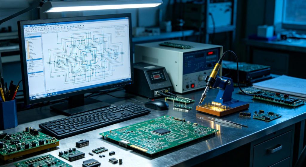
Master mainstream EDA tools first
Focus on one user-friendly, industry-recognized EDA tool to avoid scattered learning efforts. KiCad is ideal for free open-source practice, whileAltium Designer is tailored for commercial and industrial formal projects. Avoid overly complex tools such as Cadence Allegro during the initial learning phase.
Grasp basic design specifications
Master core design specifications, including trace width, clearance, via dimensions, and component placement standards. These fundamental specifications govern the manufacturability and long-term stability of all PCB designs, forming the foundation for advanced skill development.
Practice with open-source projects
Imitating mature open-source PCB layouts is the fastest way for beginners to accumulate hands-on experience. Analyze component partitioning logic, routing principles, and grounding strategies of open-source boards to build practical design intuition.
What Core Skills Do You Need to Learn PCB Layout Professionally?
Professional PCB layout learning focuses on four core competencies: standardized component placement, optimized trace routing, robust grounding design, and manufacturing-compliant optimization. These skills cover electrical performance, structural compatibility, and production feasibility, resolving the most common pain points of subpar design performance and unmanufacturable board layouts for new learners.
Reasonable component layout capability
Group components by functional modules, such as power supply, signal processing, and control circuits. Isolate heat-generating components and reserve sufficient space for assembly and heat dissipation. Strategic component placement minimizes signal interference and mitigates thermal failure risks in subsequent design stages.
Precision trace routing skills
Adhere to core routing principles: minimize signal path lengths, use 45-degree trace angles, and separate power and signal traces. Master differential pair routing, precise impedance control, and crosstalk suppression techniques for high-speed circuits to guarantee reliable signal integrity.
Standard grounding and thermal design
Implement full ground plane coverage and single-point grounding for mixed analog and digital circuits. Optimize the placement of high-power heat-generating components to prevent local overheating and board damage, enhancing overall circuit operational stability.
Design for manufacturing (DFM) awareness
All layout designs must align with actual manufacturing process capabilities. Avoid undersized vias, ultra-narrow traces, and overly dense pad layouts that fail to meet production standards, as these issues lead to mass production failures.
Which EDA Tools Are Best for Learning PCB Layout in 2026?
Selecting the right EDA tool is critical for efficient PCB layout learning. Each tool caters to distinct learning stages and industrial use cases. The following comparison outlines the ideal users, core benefits, and application scenarios of mainstream tools to help learners make informed choices.
| EDA Tool | Applicable Learning Stage | Core Advantages | Application Industries |
|---|---|---|---|
| KiCad | Beginners & Hobbyists | 100% free open-source, rich component libraries, simple operation, complete basic layout functions | Consumer Electronics, Small Industrial Control Devices |
| Altium Designer | Intermediate & Professional Designers | Powerful high-speed signal simulation, 3D preview, perfect DFM detection, industry mainstream | Automotive Electronics, Medical Electronics, Communication Equipment |
| EasyEDA | Beginners & Rapid Prototyping | Online cloud operation, no installation required, one-click manufacturing docking, fast iteration | Student Projects, Consumer Electronic Prototypes |
| Cadence Allegro | Advanced Professional Engineers | Ultra-high precision, suitable for multi-layer high-speed boards, strong industrial reliability | Aerospace, Server, High-end Communication Equipment |
What Common PCB Layout Mistakes Should Learners Avoid?
Most new PCB layout learners repeatedly make design mistakes that cause circuit instability or manufacturing failures. Identifying and avoiding these common errors boosts learning efficiency and design pass rates, which is indispensable for anyone looking to learn PCB layout proficiently.
Improper trace routing errors
Right-angle traces and long parallel high-speed traces are two prevalent novice errors. Right-angle traces trigger signal reflection, while extended parallel trace routing causes severe crosstalk, undermining overall circuit signal stability.
Unreasonable component placement
Intermingling analog and digital components or overcrowding heat-generating parts leads to severe signal interference and inadequate heat dissipation. Unstructured component layout is a leading cause of circuit functional failure in prototype designs.
Ignoring DFM design rules
Designs with insufficient component spacing, irregular vias, or no reserved assembly space result in unmanufacturable PCBs. Many novice designs perform well in simulation but fail during mass production due to neglected DFM rules.
Defective grounding design
Incomplete ground plane coverage and improper mixed grounding for analog and digital circuits introduce excessive noise interference, reducing the anti-interference capability of the entire circuit system.
How to Learn High-Speed PCB Layout Design Efficiently?
High-speed PCB layout is an advanced subset of PCB layout learning, focusing on resolving signal integrity and impedance matching issues for high-frequency circuits. Learners must master targeted optimization techniques based on foundational layout skills to meet high-end industrial design requirements.
Master impedance matching rules
Adjust trace width, dielectric thickness, and via parameters based on high-frequency signal specifications to achieve precise impedance matching. This practice effectively eliminates signal reflection and attenuation during high-speed data transmission.
Optimize differential pair routing
Maintain equal length, parallel alignment, and consistent spacing for all differential traces. Avoid trace stubs and unnecessary vias on high-speed differential lines to ensure stable and reliable high-speed signal transmission.
Strengthen crosstalk suppression design
Follow the 3W spacing principle for high-speed signals, partition high-speed and low-speed signal zones, and implement ground isolation to minimize inter-trace crosstalk and enhance circuit anti-interference performance.
What Industry PCB Layout Cases Help Improve Learning Outcomes?
Studying real-world industry-specific PCB layout cases is the most effective method to convert theoretical knowledge into practical design capabilities. Below are four high-demand industrial sectors with detailed layout guidelines and problem-solving strategies to help learners master scenario-based layout skills.
Automotive Electronics PCB Layout Case
Automotive electronic PCBs are deployed in vehicle control units, ADAS modules, and in-vehicle entertainment systems. These boards are engineered to withstand vibration, extreme temperature fluctuations, and intense electromagnetic interference in automotive environments. Key layout practices include modular power and signal circuit isolation and strict EMC compliance design.
Medical Electronics PCB Layout Case
Medical-grade PCBs are integrated into blood pressure monitors, electrocardiographs, and portable diagnostic devices. They address strict industry pain points for ultra-low noise and high signal accuracy. Layout design requires isolating weak physiological signal traces from power-induced noise while meeting medical-grade insulation and long-term stability standards.
Industrial Control PCB Layout Case
Industrial control PCBs power PLC controllers, sensor acquisition modules, and automated manufacturing equipment. They are designed to resist strong on-site electromagnetic interference and support long-term continuous operation. Core layout optimizations include thickened power traces, comprehensive grounding protection, and specialized anti-interference routing.
Communication Equipment PCB Layout Case
Communication equipment PCBs are used in 5G modules, network routers, and signal transmission hardware. They resolve critical high-speed signal transmission and impedance stability challenges. Layout design demands precise differential pair consistency, accurate impedance control, and radio frequency signal isolation to guarantee uninterrupted communication performance.
How to Balance PCB Layout Performance and Manufacturability?
High-quality PCB layout design balances electrical performance, structural compatibility, and mass production feasibility. Many new designers prioritize theoretical performance while overlooking manufacturing constraints, resulting in high-cost or non-producible board designs.
Prioritize core performance requirements
For high-speed and high-precision devices, prioritize signal integrity and operational stability as the primary design goals. Optimize layout structures to meet strict performance benchmarks without overcomplicating production processes.
Simplify redundant design for mass production
For high-volume consumer electronic products, simplify complex vias and ultra-precision layout structures. This reduces manufacturing difficulty and overall costs while maintaining essential product performance standards.
Verify design feasibility in advance
Run professional DFM validation checks before finalizing any PCB design. This proactive step eliminates potential manufacturing obstacles and achieves an optimal balance between design performance and producibility.
Thindry supports on-demand customization and provides free DFM reports for all PCB and PCBA projects. We help designers verify layout manufacturability in advance, eliminate design rework, and accelerate project delivery timelines.
How to Practice PCB Layout to Improve Skills Rapidly?
Structured hands-on practice is the fastest way to master how to learn PCB layout effectively. Passive theoretical learning alone cannot resolve real-world design challenges. Targeted progressive practice improves design proficiency and practical problem-solving capabilities significantly.
Start with single-layer and double-layer board practice
Beginners should start with single-layer power boards and double-layer signal boards. Familiarize yourself with basic routing, component placement, and grounding logic to build a solid foundation for advanced multi-layer board design.
Imitate and optimize open-source projects
Select mature open-source PCB projects for industrial and consumer electronics applications. Replicate the original layout first, then iterate and optimize routing and placement schemes to cultivate independent design thinking.
Accumulate problem-solving experience
Document every design error and its root cause, along with corresponding optimization solutions. This habit prevents repeated mistakes and continuously refines your PCB layout expertise over time.
What Are the Best PCB Layout Standards and Rules to Follow?
Standardized design rules form the backbone of high-quality PCB layout. Learning and applying universal industry standards ensures design compliance, enhances board operational stability, and adapts designs to diverse industrial application scenarios.
Electrical performance standards
Adhere to industry specifications for trace width current carrying capacity, spacing-based anti-interference, and precision impedance matching. These standards guarantee stable circuit operation under rated voltage and current conditions.
Structural assembly standards
Reserve adequate assembly clearance for all components and standardize connector placement positions to avoid structural interference during product assembly and end-user operation.
Industrial compliance standards
Different industries enforce unique compliance standards: medical electronics follow ISO 13485, automotive electronics adhere to AEC-Q series specifications, and industrial control boards comply with strict EMC anti-interference regulations.
How to Fix Common PCB Layout Performance Issues?
Designers frequently encounter performance defects during PCB layout work. Targeted troubleshooting and optimization methods can quickly resolve common issues and elevate overall PCB design quality.
Solve signal crosstalk and noise problems
Expand spacing between high-speed signal traces, add ground isolation strips, and implement full ground plane coverage. Reducing parallel routing lengths effectively suppresses crosstalk and ambient noise interference.
Solve circuit overheating problems
Disperse high-power heat-generating components evenly, increase copper pour areas for heat dissipation, and avoid clustered heat source placement. Optimize via distribution to accelerate thermal conduction and reduce overheating risks.
Solve unstable power supply problems
Place filter capacitors close to component power pins, widen power delivery traces, and separate analog and digital power domains. These adjustments eliminate voltage fluctuations and power supply noise.
FAQ: Frequently Asked Questions About Learning PCB Layout
The following high-frequency questions are curated from real learning pain points shared by PCB layout learners. All answers deliver direct, actionable solutions to resolve confusion for beginner and intermediate designers.
Is PCB Layout hard to learn for total beginners?
PCB layout is accessible for total beginners with structured, systematic learning. The entry barrier is relatively low, and proficiency depends on mastering standardized workflows and basic design rules. Difficulty only increases with advanced high-speed and multi-layer board design. Step-by-step hands-on practice allows new learners to build competence rapidly.
How long does it take to learn professional PCB layout?
Beginners can master single and double-layer PCB layout fundamentals within 1 to 2 months. 3 to 6 months of consistent practical project experience is required to achieve proficiency in standard industrial board design. Advanced high-speed layout expertise requires a minimum of one year of targeted specialized practice.
Do I need to master circuit theory before learning PCB layout?
Basic circuit theory knowledge is a prerequisite for PCB layout learning. Learners must understand component functions, fundamental circuit operating principles, and core electrical characteristics. Advanced circuit theory can be gradually acquired through ongoing layout practice.
Which is better for learning PCB layout: KiCad or Altium Designer?
KiCad is ideal for beginner training and personal practice thanks to its free open-source licensing and intuitive interface. Altium Designer is better suited for professional commercial projects and workplace applications. New learners can start with KiCad and transition to professional commercial tools after accumulating foundational experience.
What is the biggest barrier to learning advanced PCB layout?
The biggest barrier to mastering advanced PCB layout is insufficient practical experience with signal integrity optimization, impedance control, and DFM validation. Advanced layout design requires integrating electrical theory, manufacturing technology, and industry-specific scenario requirements, which demands long-term project accumulation.
Can I learn PCB layout only by watching tutorials without practical operation?
Watching tutorials alone cannot help you master professional PCB layout skills. PCB layout is a highly practical engineering skill. Only consistent hands-on practice, iterative error correction, and design optimization can develop independent professional design capabilities.
How to Take PCB Layout Skills from Beginner to Professional Level?
Elevating your PCB layout skills from beginner to professional level requires progressive learning and continuous project accumulation. Building a complete design system covering layout design, performance verification, and manufacturing optimization is the key to professional growth, enabling you to thoroughly master how to learn PCB layout in a systematic way.
First, solidify foundational EDA tool operation and standard design rules to eliminate errors in conventional layout projects. Second, accumulate cross-industry project experience to master differentiated design requirements for diverse application scenarios. Finally, learn advanced high-speed signal simulation, impedance tuning, and EMC optimization techniques to solve complex engineering challenges.
If you require customized PCB layout design, rapid prototyping, or mass production services, Thindry delivers reliable one-stop professional solutions. We support on-demand customization and provide free DFM reports for all projects to help you avoid design flaws and manufacturing risks. Reach out to our expert team via email: sales@pcbtry.com to obtain tailored solutions and place your orders.


0 Comments