
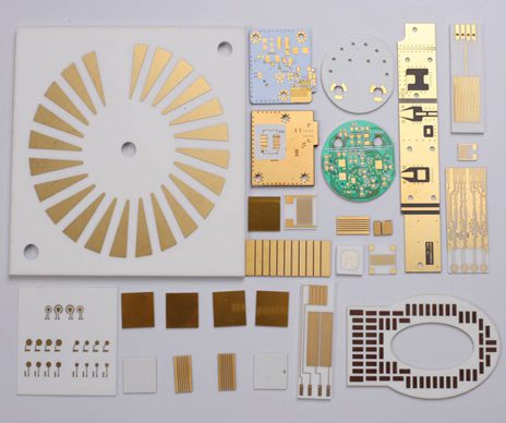


As a Ceramic PCB manufacturer with 20 years of hands-on experience, I’ve witnessed the rise of this high-performance circuit board in the electronics industry. A Ceramic PCB, or ceramic printed circuit board, uses ceramic materials as its substrate. Thanks to its excellent thermal conductivity, superior electrical insulation, and outstanding mechanical strength, it has become a core component in high-end fields such as automotive electronics, aerospace, and medical equipment. Now, let me introduce every aspect of Ceramic PCBs in detail, along with the professional services we offer.
What is a Ceramic PCB?
A Ceramic PCB is a printed circuit board that creates circuit patterns on a ceramic substrate through special processes. Compared with traditional PCBs, the ceramic substrate endows it with higher stability and reliability. It stands out in high-end electronic applications with three major advantages: extremely high thermal conductivity that rapidly dissipates heat generated by high-power devices, ensuring stable device operation; excellent insulation performance that effectively reduces signal interference and guarantees circuit stability; and remarkable mechanical strength that enables it to work reliably in harsh environments with extreme temperatures and vibrations.
Ceramic PCB Materials
Ceramic substrate materials form the basis of a Ceramic PCB’s performance, and different materials suit various scenarios:
- Alumina (Al₂O₃) Ceramic: Cost-effective and widely used in industrial control, consumer electronics, and other fields with moderate performance requirements.
- Aluminum Nitride (AlN) Ceramic: With a thermal conductivity as high as 170 – 230 W/(m·K) and a low dielectric constant, it’s the ideal choice for high-performance scenarios such as 5G communication and new energy vehicle drive modules.
- Beryllium Oxide (BeO) Ceramic: Although it has excellent thermal conductivity, its application is relatively limited due to toxicity concerns.
Our factory always stocks a variety of high-quality ceramic materials and can precisely match the most suitable material solutions according to customers’ project requirements.
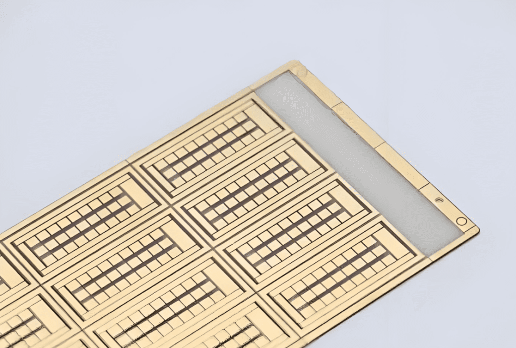
Ceramic Multilayer PCBs
Ceramic multilayer PCBs adopt advanced three-dimensional circuit architecture designs. Through precise stacking technology and high-temperature co-firing processes (HTCC), they achieve high-density circuit integration. This technology can connect dozens of circuit layers within a limited space, significantly improving the circuit wiring density and signal transmission performance per unit area. For example, in aerospace navigation systems, ceramic multilayer PCBs optimize the equipment’s space layout through highly integrated signal processing modules. Meanwhile, relying on the excellent dielectric properties of ceramic-based materials, they enhance the system’s electromagnetic compatibility (EMC) and ensure stable signal transmission.
Our Services
Ceramic PCB Design
Our design team consists of experienced engineers, each with over 15 years of industry experience. They are proficient in key technologies such as thermal stress analysis and signal integrity design for Ceramic PCBs. We strictly control every step, from schematic design to PCB layout. We once successfully optimized a customer’s design, increasing product performance by 40% and shortening the R&D cycle by 30%, helping the customer gain a competitive edge in the market.
Ceramic PCB Prototyping
Equipped with advanced ceramic processing equipment, we support ultra-fast prototyping services, with the fastest turnaround time of 24 hours. We pay meticulous attention to every process, from material cutting, pattern transfer to metallization, ensuring that the prototype fully meets the design requirements. This helps customers quickly verify product feasibility and accelerate the product development process.
Mass Production
We have a modern production base of 6,000 square meters and a monthly production capacity of over 200,000 square feet. With multiple authoritative certifications such as ISO13085 and IATF16949, and standardized production processes, we ensure consistent product quality regardless of order size, providing customers with reliable large-scale production services.
Ceramic PCB Assembly
With more than 10 professional SMT production lines, we support complex packaging processes such as BGA and QFN. We offer one-stop services including component procurement, DFM inspection, and functional testing, truly achieving seamless integration from design to finished products, saving customers time and effort.
Why Choose Us?
Twenty years of industry experience have enabled us to accumulate rich practical experience and profound technical expertise. Our independently developed ceramic metallization process can reduce production costs by 30%, providing customers with cost-effective solutions. We have established a comprehensive quality control system, and each board undergoes 12 strict inspection processes to ensure product quality. Additionally, we provide 24/7 rapid response services to solve customer problems at any time. Choosing us means choosing peace of mind, reliability, and assurance.
Advantages of Ceramic PCBs
1.Superior Heat Dissipation: Its thermal conductivity is 20 times higher than that of traditional PCBs, effectively preventing high-power devices from overheating and extending device lifespan.
2.Excellent Electrical Insulation: High-grade insulation properties ensure stable circuit operation, reducing signal interference and enhancing overall reliability.
3.High Mechanical Strength: Resistant to impacts, vibrations, and capable of operating in extreme temperatures, it’s an ideal choice for aerospace and automotive applications.
4.Long Durability: Outstanding chemical stability provides excellent corrosion resistance, significantly extending the product’s service life.
5.Fine-pitch Wiring Capability: Supports minimum line widths as low as 50μm, meeting the high-density circuit requirements of advanced technologies such as 5G and AI.
Ceramic PCB Production Process
1.Substrate Preprocessing: Use high-precision grinding equipment to control the surface flatness error of the ceramic substrate within 0.01mm, followed by deep cleaning to remove impurities, laying a solid foundation for subsequent processes.
2.Laser Drilling and Pattern Transfer: Utilize ultraviolet lasers to create tiny vias on the ceramic substrate, then transfer the circuit patterns precisely onto the substrate surface through photolithography.
3.Metallization: Apply thick-film printing or thin-film sputtering processes to form highly adhesive metal traces on the ceramic surface, endowing the substrate with conductivity.
4.Multilayer Stacking and Co-firing: Precisely align multiple ceramic substrates with circuit patterns and co-fire them in a 1,600℃ high-temperature furnace, tightly bonding the ceramic and metal into an integrated structure.
5.Inspection and Packaging: Conduct multiple strict tests on the finished products, including continuity tests, insulation tests, and reliability tests. After ensuring compliance with quality standards, perform surface coating and mechanical processing to complete the final packaging.
Each production process is monitored by professional quality inspectors in real-time. Online detection equipment dynamically adjusts key parameters to ensure high precision and stability throughout the production process. We continuously invest in research and development and optimize process details, committed to providing customers with higher-quality and more efficient Ceramic PCB products.
Problems Solved by Ceramic PCBs
1.Heat Dissipation Challenges: When high-power electronic devices operate, traditional PCBs often suffer from performance degradation or frequent failures due to heat dissipation bottlenecks. Ceramic PCBs, with their ultra-high thermal conductivity, can reduce the junction temperature of key chips by over 30%. Through efficient heat conduction path designs, they quickly disperse heat to radiators, completely eliminating the risk of thermal runaway.
2.Reliability Issues: In application scenarios with high reliability requirements, such as aerospace and automotive electronics, Ceramic PCBs demonstrate excellent environmental tolerance. With a flexural strength of over 400 MPa and a wide operating temperature range from -55℃ to 850℃, combined with the dense structure achieved by the multilayer co-firing process, they can reduce system failure rates by 80%. They ensure signal integrity and stable power transmission even in environments with severe vibrations and extreme temperature differences.
Ceramic PCB Design Guidelines
1.Thermal Expansion Coefficient Matching: Strictly control the difference in thermal expansion coefficients (CTE) between the ceramic substrate and chips within ±1ppm/℃. Through precise material selection and thermal stress simulation analysis, avoid the risk of ceramic substrate cracking caused by thermal mismatch, ensuring the reliability and stable performance of products throughout their life cycles.
2.Circuit Layout Optimization: Based on signal integrity theory, use rounded corners instead of sharp angles for wiring to effectively reduce stress concentration. Prioritize blind and buried via interconnection technologies to shorten signal transmission paths and reduce signal loss caused by parasitic parameters. Through hierarchical planning of power and ground layers and impedance matching designs, construct a low-noise and high-stability power distribution network.
3.Design for Manufacturability: According to the processing equipment precision of the manufacturing enterprise (such as the minimum aperture of laser drilling machines and the line width resolution of lithography equipment) and process capabilities (such as electroplating via filling processes and surface treatment technologies), systematically verify and design key parameters such as via size, line width, line spacing, and minimum spacing. Ensure that the design scheme seamlessly connects with mass production processes, achieving efficient transformation from design to manufacturing.
Ceramic PCB vs FR4
Ceramic PCBs and FR4 differ significantly in multiple aspects, determining their different application directions:
•Material Positioning: FR4 is a common printed circuit board material widely used in the consumer electronics field, meeting basic daily needs. In contrast, Ceramic PCBs are designed specifically for high-end applications.
•Performance Comparison: The thermal conductivity of Ceramic PCBs is 20 times higher than that of FR4, the insulation resistance is increased by three orders of magnitude, and the mechanical strength far exceeds that of FR4.
•Cost and Application: Although FR4 is more cost-effective, it cannot match Ceramic PCBs in terms of high-temperature resistance, interference immunity, and reliability. Ceramic PCBs are irreplaceable in high-end fields such as aerospace and medical equipment.
Application Fields of Ceramic PCBs
1.New Energy Vehicles: Applied in battery management systems and motor controllers to ensure efficient power transmission and stable control, enhancing vehicle performance and safety.
2.5G Communication: Used in base station power amplifiers and RF modules to meet the high-speed signal transmission and heat dissipation requirements of 5G networks.
3.Medical Equipment: Integrated into medical devices such as CT scanners and pacemakers, providing high-reliability support for precise medical procedures.
4.Aerospace: Applied in satellite communication and missile guidance systems, withstanding extreme environments and ensuring stable signal transmission.
Whether you are in the product research and development stage and need quick prototyping verification or are ready for mass production, we can provide you with one-stop solutions. Twenty years of focus and accumulation have enabled us to better understand your needs. Don’t let your excellent product ideas stay on the drawing board. Contact us immediately at sales@pcbtry.com and embark on an outstanding journey with Ceramic PCBs together!