




The PTFE dielectric constant used in a PCB design is not one universal number. Pure PTFE has low permittivity, but commercial microwave laminates combine PTFE with woven glass or ceramic fillers to control dielectric constant, loss, dimensional behavior and processing. The correct Dk is the material grade’s design value at the relevant frequency and test method—not a generic value copied from a chemistry table.
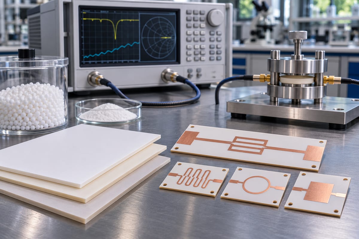
What Does Dielectric Constant Mean for a PTFE PCB?
Relative permittivity, often called Dk in PCB work, describes how a dielectric stores electric-field energy compared with vacuum. It influences transmission-line impedance, propagation delay, wavelength and resonator dimensions. It does not independently define loss; dissipation factor, conductor roughness, copper geometry and radiation also matter.
Detailed PTFE Laminate Dk Parameters
Representative Rogers product-selector values illustrate why the exact grade is essential. Values are typical supplier data at stated conditions, not finished-board guarantees.
| Material example | Construction | Typical Dk at 10 GHz | Design implication |
|---|---|---|---|
| RO3003G2 | Ceramic-filled PTFE | Process 3.00 ±0.04; design value listed separately | Low-Dk microwave routing with grade-specific modeling |
| RO3003 | Ceramic-filled PTFE | Process 3.00 ±0.04 | Do not assume its design Dk equals another 3.0 laminate |
| RO3203 | Ceramic/PTFE with woven glass | About 3.02 typical | Reinforcement changes anisotropy and processing |
| AD255C | Fluoropolymer/ceramic/glass system | Supplier nominal 2.55 | Requires its own thickness and Dk model |
Why Published Dk Values Differ
- Material composition: ceramic filler and glass reinforcement change effective permittivity.
- Frequency: measured response and extraction can vary across the band.
- Test method: clamped stripline, resonance and other methods do not produce interchangeable numbers.
- Direction: anisotropic constructions can have different in-plane and through-thickness behavior.
- Manufactured geometry: resin distribution, pressed thickness and copper treatment affect the effective circuit result.
Process Dk vs Design Dk
| Value | Purpose | How to use it |
|---|---|---|
| Specification/process Dk | Material quality control under a defined test | Use for conformance only as the datasheet directs |
| Design Dk | Better correlation with a transmission-line model | Use with the supplier’s stated frequency/method and field solver |
| Effective Dk | Describes a particular line structure | Depends on geometry and field distribution; not a raw material constant |
| Extracted Dk | Fits measured coupon behavior | Keep fixture, copper and model assumptions documented |
PTFE vs Hydrocarbon-Ceramic vs FR-4
| Material family | Main strength | Trade-off | Typical selection reason |
|---|---|---|---|
| PTFE-based RF laminate | Low loss and stable microwave options | Special processing and mechanical behavior | High-frequency loss or phase control |
| Hydrocarbon-ceramic RF laminate | RF performance with more conventional processing | Properties differ by grade and temperature | Cost/process balance |
| FR-4 | Broad availability and economical multilayers | Higher loss and wider Dk variation at RF | Lower-frequency or cost-driven sections |
How to Choose the Dk for Simulation
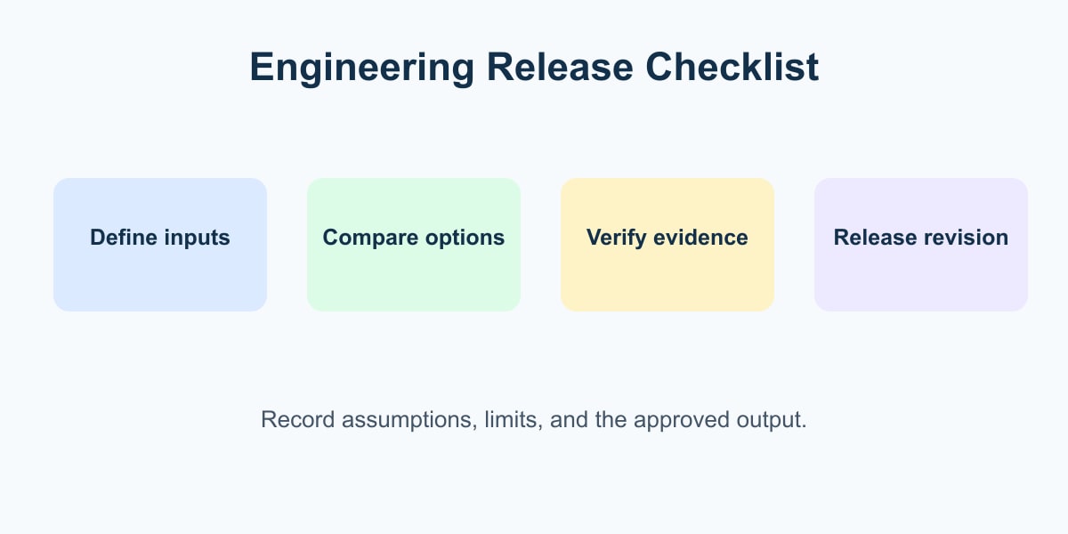
- Fix the exact laminate grade and thickness.
- Read both process and design Dk notes in the current datasheet.
- Match frequency and test direction to the application.
- Use finished copper and pressed dielectric geometry.
- Model solder mask, copper roughness and anisotropy when their effect matters.
- Correlate critical lines with a controlled coupon or resonator.
Manufacturing and Impedance Checks
Impedance depends on finished line width, copper thickness, dielectric height and material behavior. Ask the fabricator to calculate against the proposed production stackup, then control the coupon and measurement plan. Substituting a “similar Dk” laminate without reviewing loss, thickness availability, reinforcement and processing can move both impedance and insertion loss.
For multilayer RF boards, also confirm which core and bond-ply materials surround each controlled line. A PTFE core paired with a different bonding system creates a composite electromagnetic structure. The field solver should therefore use the complete layer construction rather than assigning one Dk to the entire board. Record the material revision and supplier datasheet used for the released calculation.
Common Errors
- Using 2.1 for every PTFE-based laminate.
- Mixing a datasheet process Dk with a design-Dk field-solver model.
- Ignoring test frequency and direction.
- Equating dielectric constant with dissipation factor.
- Changing laminate grade after layout without recalculating geometry.
FAQ
Is PTFE Dk always 2.1?
No. That value is associated with unfilled PTFE references; PCB laminates use fillers and reinforcement that create grade-specific values.
Does lower Dk always mean lower loss?
No. Dk and loss tangent are different properties. Copper loss, roughness and circuit geometry also contribute.
Can two materials with the same nominal Dk be substituted?
Not automatically. Compare test method, thickness, tolerance, loss, reinforcement, thermal behavior and fabrication process.
What should an RFQ include?
Provide exact material, thickness, copper, stackup, frequency, impedance targets, tolerances, quantity and required coupon/test reports.
Sources
- Rogers: High Frequency Electronics Product Selector
- Rogers: Low-loss RF microwave laminate properties
For a PTFE-based PCB material and stackup review, send the files and requirements to sales@pcbtry.com.

0 Comments